


Reaction Module (REACM)
MPC5644A Microcontroller Reference Manual, Rev. 6
724
Freescale Semiconductor
overrun condition occurs, indicating that at least one ADC data was lost (the input data that caused the
overrun is lost).
The following situations can generate an input overrun:
•
Two consecutive sample data are received from ADC or from CPU.
•
ADC and CPU sending sample data at the same time (asynchronous events).
•
Input buffer is holding sample data that are being processed by some channel and a new sample is
received from ADC or CPU (normal mode of operation).
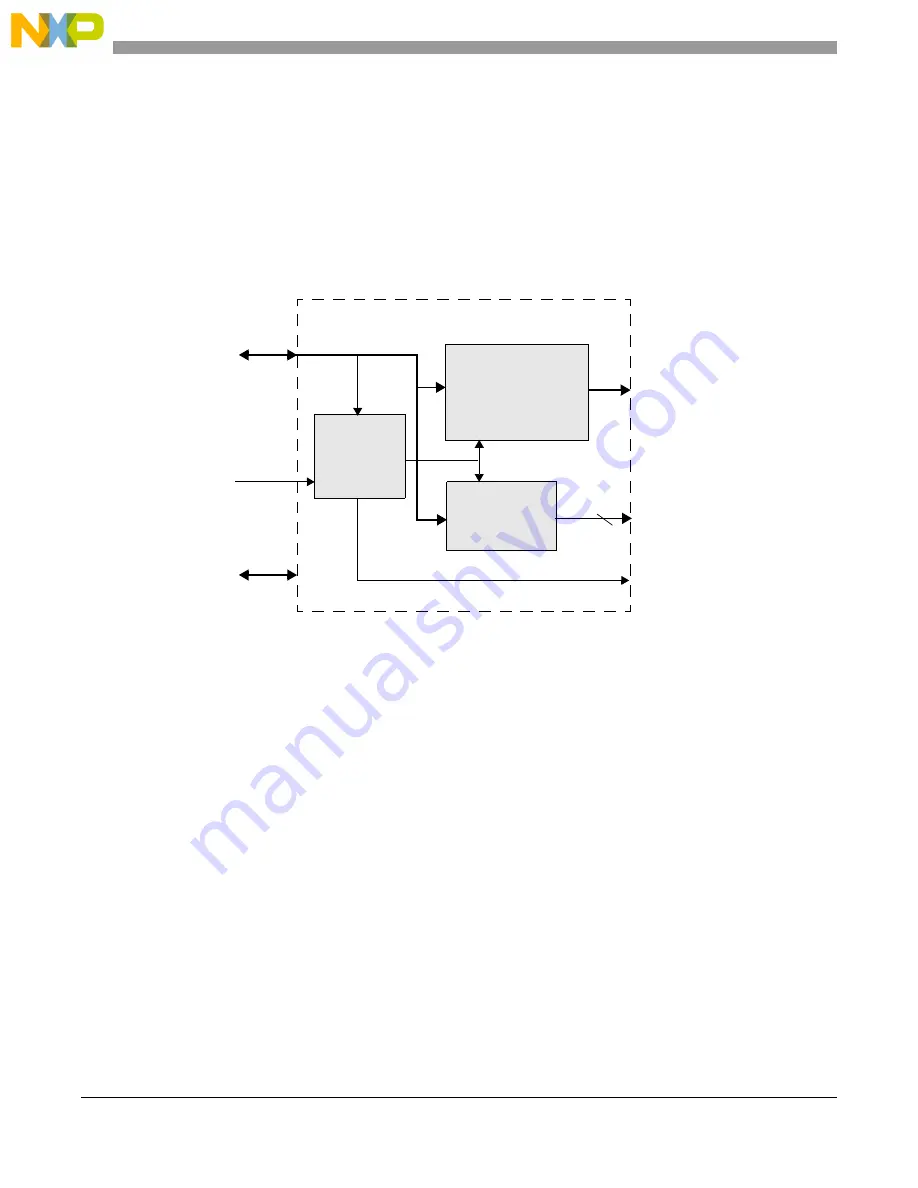
Figure 23-24. ADC interface block diagram
The maximum throughput supported by the reaction module depends upon the TAG of the incoming ADC
data. If only one reaction channel is addressed by the ADC TAG then the maximum supported ADC data
rate is one sample each five clock cycles. If two reaction channels are addressed by the same ADC TAG,
thus having the same CHRRn ADCR field, and are active at the same time, the maximum supported rate
is one ADC data on each 10 clock cycles. In general if (n) channels share the same TAG and are active at
the same time the maximum supported ADC data rate is 5×(n) clock cycles.
These limitations are related to the sharing of internal reaction module resources such as the Modulation
Word bank. The ADC conversion data should remain stable in the ADC interface until it is used by all
channels which matching TAG and CHRRn ADCR fields.
Note that if all active channels have different CHRRn ADCR fields, that is, are assigned to different TAGs,
the maximum supported ADC rate is five clock cycles. If multiple channels have the same CHRRn ADCR
field but only one is active at a time, then the maximum supported ADC data rate is also five clock cycles.
23.4.6.2
On-the-fly ADC data acquisition
The ADC interface and the threshold bank can operate in a learn mode, meaning that the received ADC
result can be stored in the threshold bank and used for comparisons. This functionality allows the user to
ADC_RESULT
ADC_TAG
ADC Interface
Control
PSI Bus
ADC result for the
Connected to all
Ack
comparison in the
threshold bank
submodule
from eQADC
New result received
4
connected to all channels
reaction channels
XBAR Master
or eTPU
Summary of Contents for MPC5644A
Page 2: ...MPC5644A Microcontroller Reference Manual Rev 6 2 Freescale Semiconductor...
Page 24: ...MPC5644A Microcontroller Reference Manual Rev 6 24 Freescale Semiconductor...
Page 26: ...MPC5644A Microcontroller Reference Manual Rev 6 26 Freescale Semiconductor...
Page 52: ...Introduction MPC5644A Microcontroller Reference Manual Rev 6 52 Freescale Semiconductor...
Page 56: ...Memory Map MPC5644A Microcontroller Reference Manual Rev 6 56 Freescale Semiconductor...
Page 1228: ...Decimation Filter MPC5644A Microcontroller Reference Manual Rev 6 1228 Freescale Semiconductor...
Page 1440: ...FlexCAN Module MPC5644A Microcontroller Reference Manual Rev 6 1440 Freescale Semiconductor...