


camisp-005
cam_hs
cam_vs
cam_pclk
camspi-006
cam_pclk
cam_vs
cam_hs
cam_d
Data 0
Data 1
Data 2
Public Version
Camera ISP Environment
www.ti.com
6.2.4 Camera ISP Protocols and Data Formats
6.2.4.1
Camera ISP Parallel Generic Configuration Protocol and Data Format (8, 10, 11, 12 Bits)
The SYNC mode implements a generic parallel interface with the image sensor. The SYNC mode
supports 8 to 12-bit-wide data signals.
In this configuration, no assumptions are made on the data format of pixels, but the dynamic range is
limited to 8-, 10-, 12 bit (data can be pure luminance for black and white sensor, RGB444, Bayer RGB,
etc.). The pixel data is presented on cam_d, where one pixel is sampled for every cam_pclk rising edge
(or falling edge, depending on the configuration of cam_pclk polarity). For more information, see
.
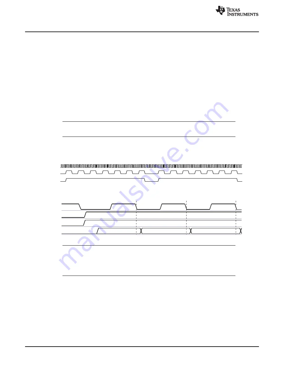
Additional pixel times between rows represent blanking periods. Active pixels are identified by a
combination of two additional timing signals: horizontal synchronization (cam_hs) and vertical
synchronization (cam_vs). During the image-sensor readout, these signals define when a row of valid data
begins and ends, and when a frame starts and ends.
NOTE:
For correct operation, the clock cam_pclk must run during blanking periods (cam_hs and
cam_vs inactive). cam_pclk must start before sending cam_d and start cam_vs and cam_hs.
and
show the frame and data timing, respectively, based on synchronization signals
in the parallel No BT configuration.
Figure 6-2. Camera ISP Synchronization Signals and Frame Timing in SYNC Mode
Figure 6-3. Camera ISP Synchronization Signals and Data Timing in SYNC Mode
NOTE:
The pixel clock can be gated to qualify valid pixels. It can also be gated during blanking
periods to reduce power consumption. However, at least 4 clock pulses are required before
sending active image data and synchronization information; 8 clock pulses are required after
the end of active video. Extra-clock pulses are allowed but not required during the line
blanking periods.
shows the timing diagram of the SYNC move clock gating.
1096
Camera Image Signal Processor
SWPU177N – December 2009 – Revised November 2010
Copyright © 2009–2010, Texas Instruments Incorporated
Содержание OMAP36 Series
Страница 174: ...174 List of Tables SWPU177N December 2009 Revised November 2010 Copyright 2009 2010 Texas Instruments Incorporated ...
Страница 692: ...692 MPU Subsystem SWPU177N December 2009 Revised November 2010 Copyright 2009 2010 Texas Instruments Incorporated ...
Страница 1084: ...1084 IVA2 2 Subsystem SWPU177N December 2009 Revised November 2010 Copyright 2009 2010 Texas Instruments Incorporated ...
Страница 1990: ...1990 2D 3D Graphics Accelerator SWPU177N December 2009 Revised November 2010 Copyright 2009 2010 Texas Instruments Incorporated ...
Страница 2334: ...2334 Memory Subsystem SWPU177N December 2009 Revised November 2010 Copyright 2009 2010 Texas Instruments Incorporated ...
Страница 2700: ...2700 Memory Management Units SWPU177N December 2009 Revised November 2010 Copyright 2009 2010 Texas Instruments Incorporated ...
Страница 2868: ...2868 HDQ 1 Wire SWPU177N December 2009 Revised November 2010 Copyright 2009 2010 Texas Instruments Incorporated ...
Страница 2974: ...2974 UART IrDA CIR SWPU177N December 2009 Revised November 2010 Copyright 2009 2010 Texas Instruments Incorporated ...
Страница 3054: ...3054 Multichannel SPI SWPU177N December 2009 Revised November 2010 Copyright 2009 2010 Texas Instruments Incorporated ...
Страница 3462: ...3462 MMC SD SDIO Card Interface SWPU177N December 2009 Revised November 2010 Copyright 2009 2010 Texas Instruments Incorporated ...
Страница 3508: ...3508 General Purpose Interface SWPU177N December 2009 Revised November 2010 Copyright 2009 2010 Texas Instruments Incorporated ...
Страница 3584: ...3584 Initialization SWPU177N December 2009 Revised November 2010 Copyright 2009 2010 Texas Instruments Incorporated ...
Страница 3648: ...3648 Debug and Emulation SWPU177N December 2009 Revised November 2010 Copyright 2009 2010 Texas Instruments Incorporated ...


