DPLL<n>_ALWON_FCLK
DPLL<n>_FCLK
High-frequency
bypass clock
DPLL power mode
CLKOUT
Multiplier and divider
(M,N)
M2
M3
M4
M5
M6
Bypass clock
CLKOUT_M2
CLKOUT_M3
CLKOUT_M4
CLKOUT_M5
CLKOUT_M6
Gating control
Low-frequency
bypass clock
Hardware control
Bypass select
F
ref
prcm-102
control bit field
DPLL
PRCM
Dividers
Public Version
www.ti.com
PRCM Functional Description
3.5.3.3.3.2 Type B DPLL (Low-Jitter)
To generate high-frequency clocks, the device supports one on-chip low-jitter DPLL controlled directly by
the PRCM module:
•
DPLL4 (PER)
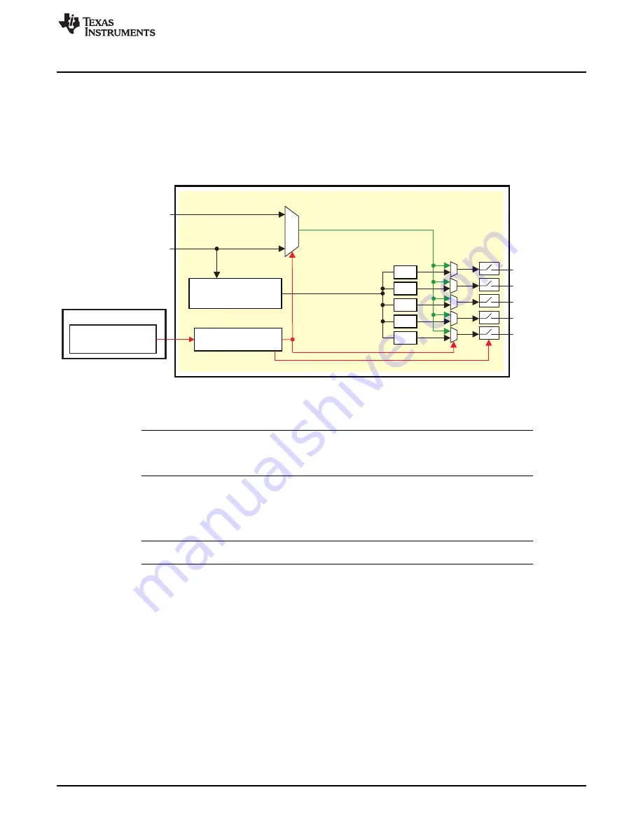
shows the functional architecture of DPLL4.
Figure 3-43. DPLL4 Functional Diagram
DPLL4 receives only one input clock from PRM module, and it is used as the reference and the bypass
clock.
NOTE:
The DPLL4 reference clock can be pre-divided before feeding the DPLL4. This is done in
the PRM thanks to a dedicated programmable register
DPLL4_CLKINP_DIV.
It internally generates one main clock according to the following equation:
•
CLKOUT = (F
ref
x M)/(N+1)
where M is a 12-bit multiplier and N is a 7-bit divider.
NOTE:
When M is set to 0 or 1, the DPLL is forced to bypass mode.
The internal clock (CLKOUT) of the DPLL can then be used to generate five independent output clocks:
•
CLKOUT_M2 = CLKOUT/M2
•
CLKOUT_M3 = CLKOUT/M3
•
CLKOUT_M4 = CLKOUT/M4
•
CLKOUT_M5 = CLKOUT/M5
•
CLKOUT_M6 = CLKOUT/M6
where M2, M3, M4, M5, and M6 are additional dividers for the DPLL-synthesized clock.
The output clock frequencies defined by these equations are generated by the DPLL only when it is
locked. When the DPLL is in bypass mode, however, all clock outputs run at the bypass clock frequency.
The bypass clock in DPLL4 can be only the low-frequency reference clock.
DPLL4 requires 2 additional settings than the other DPLLs.
•
The user must select which one of the digitally controlled oscillators (DCO) of the DPLL4 is used,
depending on the targeted lock frequency. This is done in
[23:21] DCO_SEL.
305
SWPU177N – December 2009 – Revised November 2010
Power, Reset, and Clock Management
Copyright © 2009–2010, Texas Instruments Incorporated
Содержание OMAP36 Series
Страница 174: ...174 List of Tables SWPU177N December 2009 Revised November 2010 Copyright 2009 2010 Texas Instruments Incorporated ...
Страница 692: ...692 MPU Subsystem SWPU177N December 2009 Revised November 2010 Copyright 2009 2010 Texas Instruments Incorporated ...
Страница 1084: ...1084 IVA2 2 Subsystem SWPU177N December 2009 Revised November 2010 Copyright 2009 2010 Texas Instruments Incorporated ...
Страница 1990: ...1990 2D 3D Graphics Accelerator SWPU177N December 2009 Revised November 2010 Copyright 2009 2010 Texas Instruments Incorporated ...
Страница 2334: ...2334 Memory Subsystem SWPU177N December 2009 Revised November 2010 Copyright 2009 2010 Texas Instruments Incorporated ...
Страница 2700: ...2700 Memory Management Units SWPU177N December 2009 Revised November 2010 Copyright 2009 2010 Texas Instruments Incorporated ...
Страница 2868: ...2868 HDQ 1 Wire SWPU177N December 2009 Revised November 2010 Copyright 2009 2010 Texas Instruments Incorporated ...
Страница 2974: ...2974 UART IrDA CIR SWPU177N December 2009 Revised November 2010 Copyright 2009 2010 Texas Instruments Incorporated ...
Страница 3054: ...3054 Multichannel SPI SWPU177N December 2009 Revised November 2010 Copyright 2009 2010 Texas Instruments Incorporated ...
Страница 3462: ...3462 MMC SD SDIO Card Interface SWPU177N December 2009 Revised November 2010 Copyright 2009 2010 Texas Instruments Incorporated ...
Страница 3508: ...3508 General Purpose Interface SWPU177N December 2009 Revised November 2010 Copyright 2009 2010 Texas Instruments Incorporated ...
Страница 3584: ...3584 Initialization SWPU177N December 2009 Revised November 2010 Copyright 2009 2010 Texas Instruments Incorporated ...
Страница 3648: ...3648 Debug and Emulation SWPU177N December 2009 Revised November 2010 Copyright 2009 2010 Texas Instruments Incorporated ...


