


41.5.13 PWM synchronization
The PWM synchronization provides an opportunity to update the MOD, HCR, CNTIN,
CnV, OUTMASK, INVCTRL and SWOCTRL registers with their buffered value and
force the FTM counter to the CNTIN register value.
Note
The legacy PWM synchronization (SYNCMODE = 0) is a
subset of the enhanced PWM synchronization (SYNCMODE =
1). Thus, only the enhanced PWM synchronization must be
used.
41.5.13.1 Hardware trigger
Three hardware trigger signal inputs of the FTM module are enabled when TRIGn = 1,
where n = 0, 1 or 2 corresponding to each one of the input signals, respectively. The
hardware trigger input n is synchronized by the FTM input clock. The PWM
synchronization with hardware trigger is initiated when a rising edge is detected at the
enabled hardware trigger inputs.
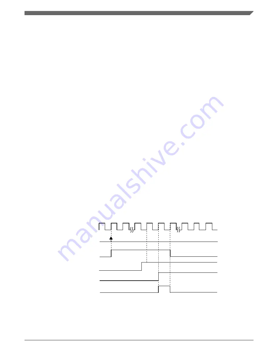
If (HWTRIGMODE = 0) then the TRIGn bit is cleared when 0 is written to it or when the
trigger n event is detected.
In this case, if two or more hardware triggers are enabled (for example, TRIG0 and
TRIG1 = 1) and only trigger 1 event occurs, then only TRIG1 bit is cleared. If a trigger n
event occurs together with a write setting TRIGn bit, then the synchronization is initiated,
but TRIGn bit remains set due to the write operation.
write 1 to TRIG0 bit
FTM input clock
synchronized trigger_0
by FTM input clock
trigger 0 event
Note
TRIG0 bit
trigger_0 input
All hardware trigger inputs have the same behavior.
Figure 41-52. Hardware trigger event with HWTRIGMODE = 0
Chapter 41 FlexTimer Module (FTM)
MWCT101xS Series Reference Manual, Rev. 3, 07/2019
NXP Semiconductors
1223
Summary of Contents for MWCT101 S Series
Page 2: ...MWCT101xS Series Reference Manual Rev 3 07 2019 2 NXP Semiconductors...
Page 42: ...MWCT101xS Series Reference Manual Rev 3 07 2019 42 NXP Semiconductors...
Page 50: ...Conventions MWCT101xS Series Reference Manual Rev 3 07 2019 50 NXP Semiconductors...
Page 70: ...Aliased bit band regions MWCT101xS Series Reference Manual Rev 3 07 2019 70 NXP Semiconductors...
Page 78: ...Pinout diagrams MWCT101xS Series Reference Manual Rev 3 07 2019 78 NXP Semiconductors...
Page 96: ...WCT101xS safety concept MWCT101xS Series Reference Manual Rev 3 07 2019 96 NXP Semiconductors...
Page 130: ...Functional description MWCT101xS Series Reference Manual Rev 3 07 2019 130 NXP Semiconductors...
Page 284: ...Functional description MWCT101xS Series Reference Manual Rev 3 07 2019 284 NXP Semiconductors...
Page 430: ...Functional Description MWCT101xS Series Reference Manual Rev 3 07 2019 430 NXP Semiconductors...
Page 472: ...Application Information MWCT101xS Series Reference Manual Rev 3 07 2019 472 NXP Semiconductors...
Page 528: ...Module clocks MWCT101xS Series Reference Manual Rev 3 07 2019 528 NXP Semiconductors...
Page 634: ...SRAM configuration MWCT101xS Series Reference Manual Rev 3 07 2019 634 NXP Semiconductors...
Page 818: ...Functional description MWCT101xS Series Reference Manual Rev 3 07 2019 818 NXP Semiconductors...
Page 960: ...Functional description MWCT101xS Series Reference Manual Rev 3 07 2019 960 NXP Semiconductors...
Page 992: ...ADC calibration scheme MWCT101xS Series Reference Manual Rev 3 07 2019 992 NXP Semiconductors...
Page 1348: ...Functional description MWCT101xS Series Reference Manual Rev 3 07 2019 1348 NXP Semiconductors...
Page 1366: ...Functional description MWCT101xS Series Reference Manual Rev 3 07 2019 1366 NXP Semiconductors...
Page 1514: ...Functional description MWCT101xS Series Reference Manual Rev 3 07 2019 1514 NXP Semiconductors...
Page 1726: ...Debug and security MWCT101xS Series Reference Manual Rev 3 07 2019 1726 NXP Semiconductors...
Page 1760: ...MWCT101xS Series Reference Manual Rev 3 07 2019 1760 NXP Semiconductors...


