


41.1.5 FTM Input Capture Options
The following channel 0 input capture source options are selected via SIM_FTMOPT1.
The external pin option is selected by default.
• FTM1 channel 0 input capture = FTM1_CH0 pin or CMP0 output
• FTM2 channel 0 input capture = FTM2_CH0 pin or CMP0 output
• FTM2 channel 1 input capture = FTM2_CH1 pin or exclusive OR of FTM2_CH0,
FTM2_CH1, and FTM1_CH1. See
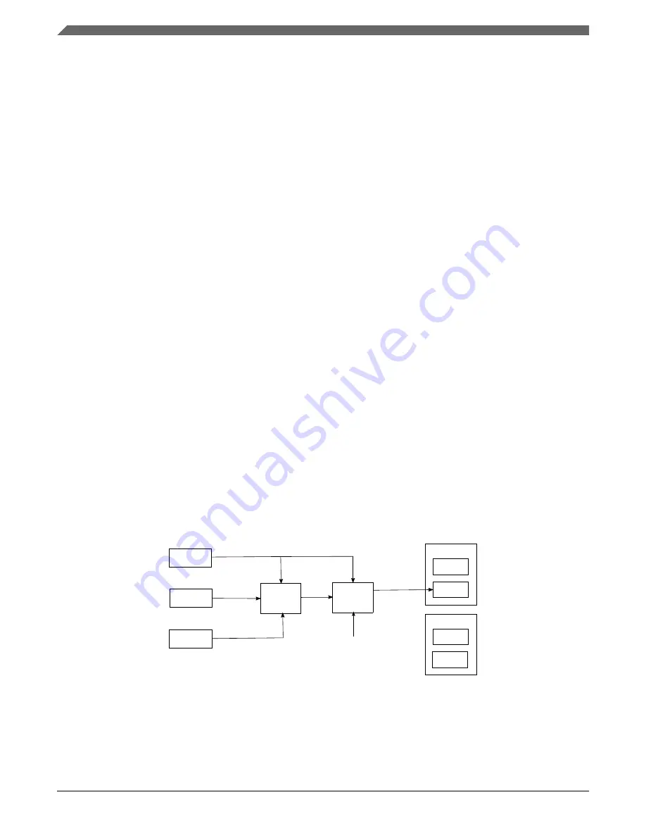
41.1.6 FTM Hall sensor support
For 3 phase motor control sensor-ed applications the use of Hall sensors, generally 3
sensors placed 120 degrees apart around the rotor, are deployed to detect position and
speed. Each of the 3 sensors provides a pulse that applied to an input capture pin, can
then be analyzed and both speed and position can be deduced. To simplify the
calculations required by the CPU on each hall sensor's input, if all 3 inputs are
"exclusively OR'd" into one timer channel and the free running counter is refreshed on
every edge then this can simplify the speed calculation.
Via the SIM module and SIM_FTMOPT1 register the FTM2CH1SEL bit provides the
choice of normal FTM2_CH1 input or the XOR of FTM2_CH0, FTM2_CH1 and
FTM1_CH1 pins that will be applied to FTM2_CH1.
NOTE
If the user utilizes FTM1_CH1 to be an input to FTM2_CH1,
FTM1_CH0 can still be utilized for other functions.
X O R
FTM2_CH1
FTM2_CH0
FTM1_CH1
Ch0
Ch1
FTM2
Ch0
Ch1
FTM1
SIM_FTMOPT1[FTM2CH1SEL]
Figure 41-3. FTM Hall Sensor Configuration
Chip-specific FTM information
MWCT101xS Series Reference Manual, Rev. 3, 07/2019
1124
NXP Semiconductors
Summary of Contents for MWCT101 S Series
Page 2: ...MWCT101xS Series Reference Manual Rev 3 07 2019 2 NXP Semiconductors...
Page 42: ...MWCT101xS Series Reference Manual Rev 3 07 2019 42 NXP Semiconductors...
Page 50: ...Conventions MWCT101xS Series Reference Manual Rev 3 07 2019 50 NXP Semiconductors...
Page 70: ...Aliased bit band regions MWCT101xS Series Reference Manual Rev 3 07 2019 70 NXP Semiconductors...
Page 78: ...Pinout diagrams MWCT101xS Series Reference Manual Rev 3 07 2019 78 NXP Semiconductors...
Page 96: ...WCT101xS safety concept MWCT101xS Series Reference Manual Rev 3 07 2019 96 NXP Semiconductors...
Page 130: ...Functional description MWCT101xS Series Reference Manual Rev 3 07 2019 130 NXP Semiconductors...
Page 284: ...Functional description MWCT101xS Series Reference Manual Rev 3 07 2019 284 NXP Semiconductors...
Page 430: ...Functional Description MWCT101xS Series Reference Manual Rev 3 07 2019 430 NXP Semiconductors...
Page 472: ...Application Information MWCT101xS Series Reference Manual Rev 3 07 2019 472 NXP Semiconductors...
Page 528: ...Module clocks MWCT101xS Series Reference Manual Rev 3 07 2019 528 NXP Semiconductors...
Page 634: ...SRAM configuration MWCT101xS Series Reference Manual Rev 3 07 2019 634 NXP Semiconductors...
Page 818: ...Functional description MWCT101xS Series Reference Manual Rev 3 07 2019 818 NXP Semiconductors...
Page 960: ...Functional description MWCT101xS Series Reference Manual Rev 3 07 2019 960 NXP Semiconductors...
Page 992: ...ADC calibration scheme MWCT101xS Series Reference Manual Rev 3 07 2019 992 NXP Semiconductors...
Page 1348: ...Functional description MWCT101xS Series Reference Manual Rev 3 07 2019 1348 NXP Semiconductors...
Page 1366: ...Functional description MWCT101xS Series Reference Manual Rev 3 07 2019 1366 NXP Semiconductors...
Page 1514: ...Functional description MWCT101xS Series Reference Manual Rev 3 07 2019 1514 NXP Semiconductors...
Page 1726: ...Debug and security MWCT101xS Series Reference Manual Rev 3 07 2019 1726 NXP Semiconductors...
Page 1760: ...MWCT101xS Series Reference Manual Rev 3 07 2019 1760 NXP Semiconductors...


