


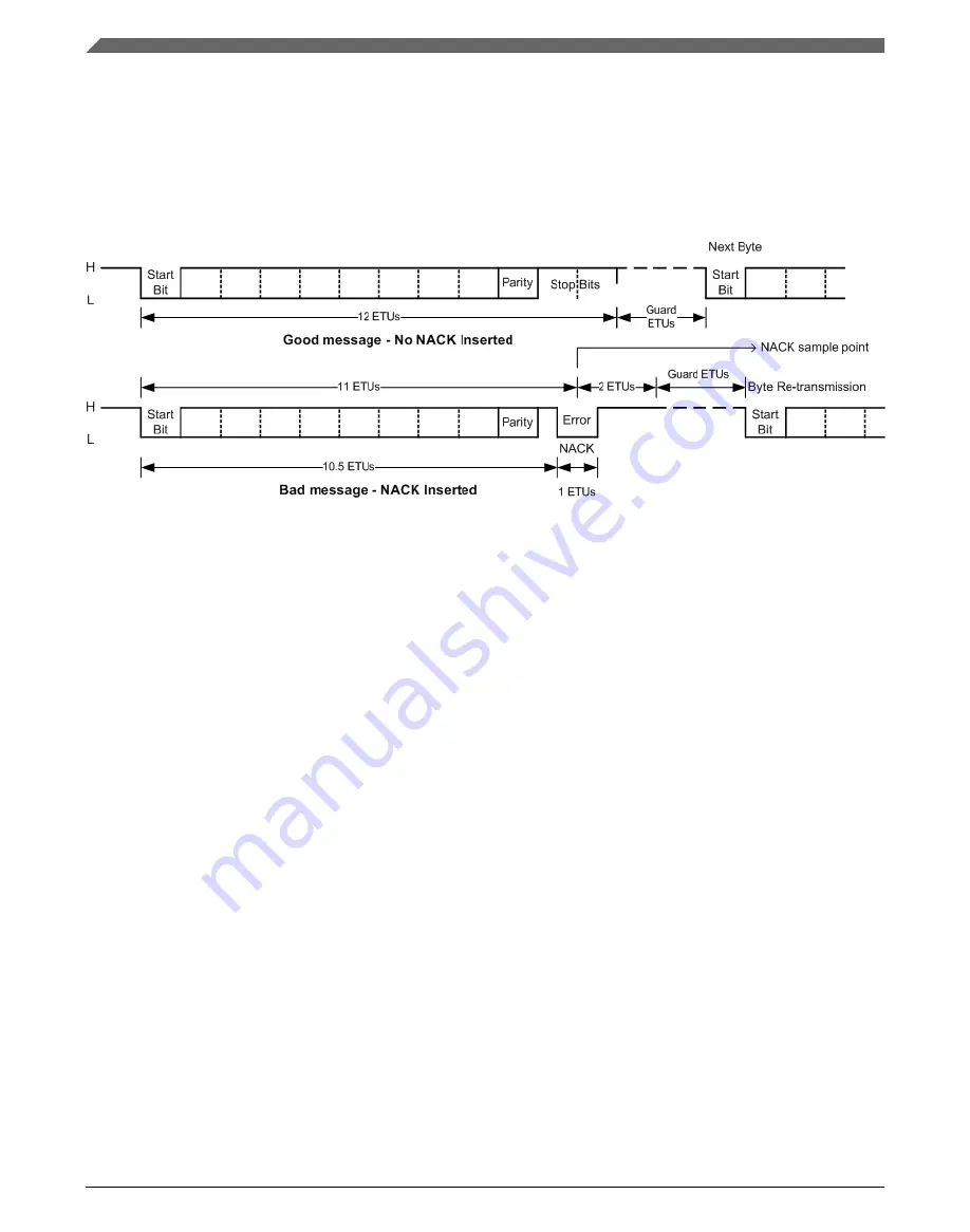
21.6.4.2 NACK Insertion
The transmitter is responsible for driving the output low during the STOP bit time to
signify an error was detected in the received data from the Smart Card. This logic
responds to a NACK request generated by the receiver block.
Figure 21-5. NACK Insertion
The NACK generation logic is also responsible for keeping track of the number of
NACKs received during a transmit operation. The receiver detects NACKs generated by
the Smart Card, and reports them to the transmit NACK logic. Once the number of
detected NACKs has reached the programmed threshold (TNCK_THD[3:0]), an interrupt
flag (TNTE) is generated, the transmit FIFO is flushed, and the transmitter is disabled.
21.6.4.3 Using EMV SIM Transmitter with "T=1" Smart Cards
The EMV SIM module provides hardware support for “T=1” type Smart Cards. These
type of cards present several requirements above and beyond the standard “T=0” cards.
The features provided to meet the requirements that pertain to the EMV SIM transmitter
are as follows:
• 11 ETU Characters
• The EMV SIM module transmitter has a programmable guard time register that
allows the programmer to specify the number of ETUs between character
transmissions. Programming a value of 255 (0xFF) in the GETU[7:0] bits in the
GUARD_CNTL register will set the number of ETUs per character transmitted
to 11.
• Character Waiting Time
• The character waiting time (CWT) is defined as the time between the start bits of
two consecutive characters. The value of CWT can range from 12 ETU to 32779
ETU. The time between transmitted characters is controlled by the
Functional Description
K32 L2A Reference Manual, Rev. 2, 01/2020
520
NXP Semiconductors
Summary of Contents for K32 L2A Series
Page 2: ...K32 L2A Reference Manual Rev 2 01 2020 2 NXP Semiconductors...
Page 42: ...K32 L2A Reference Manual Rev 2 01 2020 42 NXP Semiconductors...
Page 122: ...Flash Memory Clock K32 L2A Reference Manual Rev 2 01 2020 122 NXP Semiconductors...
Page 158: ...Debug and security K32 L2A Reference Manual Rev 2 01 2020 158 NXP Semiconductors...
Page 174: ...Module Signal Description Tables K32 L2A Reference Manual Rev 2 01 2020 174 NXP Semiconductors...
Page 246: ...Application information K32 L2A Reference Manual Rev 2 01 2020 246 NXP Semiconductors...
Page 374: ...CMP Trigger Mode K32 L2A Reference Manual Rev 2 01 2020 374 NXP Semiconductors...
Page 384: ...Functional description K32 L2A Reference Manual Rev 2 01 2020 384 NXP Semiconductors...
Page 592: ...Application Information K32 L2A Reference Manual Rev 2 01 2020 592 NXP Semiconductors...
Page 656: ...Functional Description K32 L2A Reference Manual Rev 2 01 2020 656 NXP Semiconductors...
Page 664: ...Functional Description K32 L2A Reference Manual Rev 2 01 2020 664 NXP Semiconductors...
Page 744: ...Functional description K32 L2A Reference Manual Rev 2 01 2020 744 NXP Semiconductors...
Page 762: ...Functional description K32 L2A Reference Manual Rev 2 01 2020 762 NXP Semiconductors...
Page 806: ...Functional description K32 L2A Reference Manual Rev 2 01 2020 806 NXP Semiconductors...
Page 868: ...Integer square root K32 L2A Reference Manual Rev 2 01 2020 868 NXP Semiconductors...
Page 976: ...Functional description K32 L2A Reference Manual Rev 2 01 2020 976 NXP Semiconductors...
Page 1012: ...Functional description K32 L2A Reference Manual Rev 2 01 2020 1012 NXP Semiconductors...
Page 1094: ...Functional description K32 L2A Reference Manual Rev 2 01 2020 1094 NXP Semiconductors...
Page 1132: ...Functional description K32 L2A Reference Manual Rev 2 01 2020 1132 NXP Semiconductors...
Page 1182: ...Functional description K32 L2A Reference Manual Rev 2 01 2020 1182 NXP Semiconductors...
Page 1290: ...Functional description K32 L2A Reference Manual Rev 2 01 2020 1290 NXP Semiconductors...