


Enhanced Serial Communication Interface (eSCI)
MPC5566 Microcontroller Reference Manual, Rev. 2
21-38
Freescale Semiconductor
NOTE
It is also possible to setup a whole sequence of RX and TX frames, and
generate a single event at the end of that sequence.
Refer to
for more information.
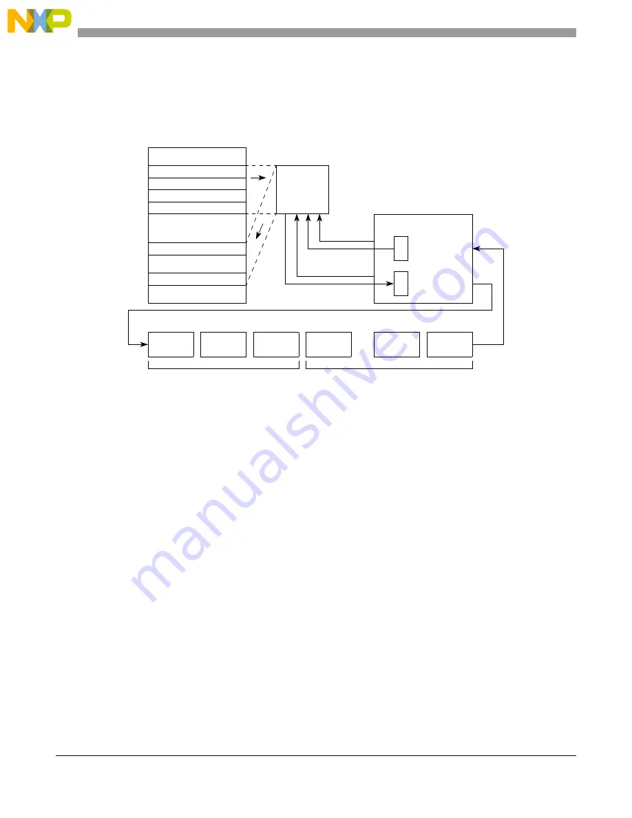
Figure 21-26. DMA Transfer of an RX frame
21.4.10.4 LIN Error Handling
The LIN hardware can detect several error conditions of the LIN protocol. LIN hardware receives all
transmitted bytes, and compares the values with expected values to determine if the data is valid. If a
mismatch occurs, a bit error is generated and the LIN FSM returns to its start state.
For an RX frame the LIN hardware can detect a slave timeout error. The exact slave timeout error value
can be set via the timeout bits in the ESCI
x
_LTR. If the frame is not complete within the number of clock
cycles specified in the register, the LIN FSM returns to its start state, and the STO interrupt is issued.
The LIN protocol supports a sleep mode. After 25,000 bus cycles of inactivity the bus is assumed to be in
sleep mode. Normally entering sleep mode can be avoided, if the LIN master is regularly creating some
bus activity. Otherwise the timeout state needs to be detected by the application software, for example by
setting a timer.
Both LIN masters and LIN slaves can cause the bus to exit sleep mode by sending a break signal. The LIN
hardware generates a break when the WU bit in the LIN control register is written. After transmitting the
break, data is not sent out (TXRDY = 0) until the wake-up period expires. Define the wakeup period using
the WUD bits in the LIN control register.
Break signals sent by a LIN slave are received by the LIN hardware, and so indicated by setting the WAKE
flag in the LIN status register.
Break
Sync
ID
Data
Data
CSum
• • •
LIN Frame
Transmit
DMA
controller
Data
n
Data 1
Timeout
Control/timeout
Length
ID
•
•
•
TX DMA
channel
LIN eSCI
Receive
From master
From slave
RX DMA
channel
register
register
Summary of Contents for MPC5566
Page 81: ...Introduction MPC5566 Microcontroller Reference Manual Rev 2 1 24 Freescale Semiconductor...
Page 135: ...Signal Description MPC5566 Microcontroller Reference Manual Rev 2 2 54 Freescale Semiconductor...
Page 189: ...Reset MPC5566 Microcontroller Reference Manual Rev 2 4 20 Freescale Semiconductor...
Page 603: ...Flash Memory MPC5566 Microcontroller Reference Manual Rev 2 13 38 Freescale Semiconductor...
Page 609: ...SRAM MPC5566 Microcontroller Reference Manual Rev 2 14 6 Freescale Semiconductor...
Page 1073: ...MPC5566 Microcontroller Reference Manual Rev 2 22 36 Freescale Semiconductor...
Page 1185: ...Nexus MPC5566 Microcontroller Reference Manual Rev 2 25 92 Freescale Semiconductor...


