


Enhanced Serial Communication Interface (eSCI)
MPC5566 Microcontroller Reference Manual, Rev. 2
Freescale Semiconductor
21-37
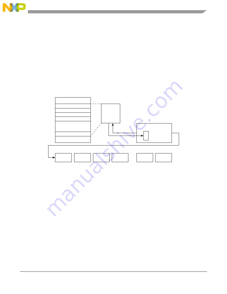
It is possible to set up a DMA channel to handle all the tasks required to send a TX frame. For this
operation, the TX DMA channel must be activated by setting the ESCI
x
_CR2[TXDMA] bit. The control
information for the LIN frame (ID, message length, TX/RX type, timeout, etc.) and the data bytes are
stored at an appropriate memory location. The DMA controller is then set up to transfer this block of
memory to a location (the ESCI
x
_LTR). After transmission is complete, either the DMA controller or the
LIN hardware can generate an interrupt to the CPU.
NOTE
In contrast to the standard software implementation where each byte
transmission requires several interrupts, the DMA controller and eSCI
handle communication, bit error and physical bus error checking,
checksum, and CRC generation (checking on the RX side).
Refer to
for more information.
Figure 21-25. DMA Transfer of a TX Frame
21.4.10.3 Generating an RX Frame
For RX frames the header information is provided by the LIN master. The data, CRC and checksum bytes
(as enabled) are provided by the LIN slave. The LIN master verifies CRC and checksum bytes transmitted
by the slave.
For an RX frame, control information must be written to the ESCI
x
_LTR in the same manner as for the
TX frames. Additionally the timeout bits, which define the time to complete the entire frame, must be
written. Then the ESCI
x
_SR[RXRDY] bit must be checked (either with an interrupt, RX DMA interface,
or by polling) to detect incoming data bytes. The checksum byte normally does not appear in the
ESCI
x
_LRR, instead the LIN hardware verifies the checksum and issue an interrupt, if the checksum value
is not correct.
Two DMA channels can be used when executing an RX frame: one to transfer the header/control
information from a memory location to the ESCI
x
_LTR, and one to transfer the incoming data bytes from
the ESCI
x
_LRR to a table in memory. After the last byte from the RX frame has been stored, the DMA
controller can indicate completion to the CPU.
Break
Sync
ID
Data
Data
CSum
• • •
LIN Frame
LIN eSCI
ESCI
x
_LTR
DMA
Controller
Data
n
Data 1
Control/Timeout
Length
ID
•
•
•
TX DMA
Channel
Summary of Contents for MPC5566
Page 81: ...Introduction MPC5566 Microcontroller Reference Manual Rev 2 1 24 Freescale Semiconductor...
Page 135: ...Signal Description MPC5566 Microcontroller Reference Manual Rev 2 2 54 Freescale Semiconductor...
Page 189: ...Reset MPC5566 Microcontroller Reference Manual Rev 2 4 20 Freescale Semiconductor...
Page 603: ...Flash Memory MPC5566 Microcontroller Reference Manual Rev 2 13 38 Freescale Semiconductor...
Page 609: ...SRAM MPC5566 Microcontroller Reference Manual Rev 2 14 6 Freescale Semiconductor...
Page 1073: ...MPC5566 Microcontroller Reference Manual Rev 2 22 36 Freescale Semiconductor...
Page 1185: ...Nexus MPC5566 Microcontroller Reference Manual Rev 2 25 92 Freescale Semiconductor...


