


S1
S2
S2
S3
S3
S4
S4
S5
S5
S6
S6
S7
S7
S8
S8
ADC0
ADC1
S1
Functional Description
709
SLAU723A – October 2017 – Revised October 2018
Copyright © 2017–2018, Texas Instruments Incorporated
Analog-to-Digital Converter (ADC)
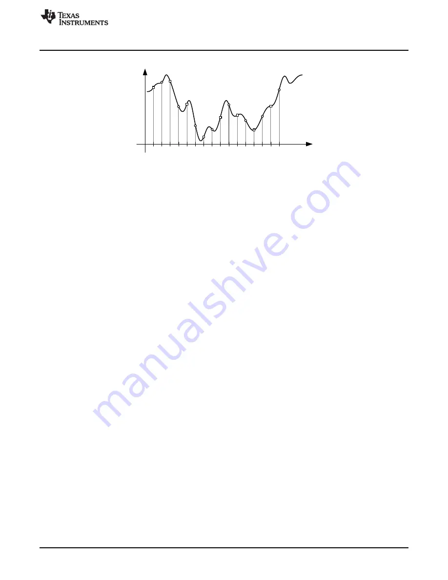
Figure 10-5. Skewed Sampling
10.3.2.7 Module Clocking
The ADC digital block is clocked by the system clock and the ADC analog block is clocked from a
separate conversion clock (ADC Clock). The ADC clock frequency can be up to 32 MHz to generate a
conversion rate of 2 Msps. A 16 MHz ADC clock provides a 1 Msps sampling rate. There are three
sources of the ADC clock:
•
Divided PLL VCO. The PLL VCO frequency can be configured to generate up to a 32-MHz clock for a
conversion rate of 2 Msps. The CS field in the ADCCC register must be programmed to 0x0 to select
the PLL VCO and the CLKDIV field is used to set the appropriate clock divisor for the desired
frequency.
•
16 MHz PIOSC. Using the PIOSC provides a conversion rate near 1 Msps. To use the PIOSC to clock
the ADC, first power up the PLL and then enable the PIOSC in the CS bit field in the ADCCC register,
then disable the PLL.
•
MOSC. The MOSC clock source must be 16 MHz for a 1 Msps conversion rate and 32 MHz for a 2
Msps conversion rate.
The system clock must be at the same frequency or higher than the ADC clock. All ADC modules share
the same clock source to facilitate the synchronization of data samples between conversion units, the
selection and programming of which is provided by the ADCCC register of ADC0. The ADC modules do
not run at different conversion rates.
10.3.2.8 Busy Status
The BUSY bit of the ADCACTSS register is used to indicate when the ADC is busy with a current
conversion. When there are no triggers pending which may start a new conversion in the immediate cycle
or next few cycles, the BUSY bit reads as 0. Software must read the status of the BUSY bit as clear
before disabling the ADC clock by writing to the ADC Run Mode Clock Gating Control (RCGCADC)
register.
10.3.3 Hardware Sample Averaging Circuit
Higher precision results can be generated using the hardware averaging circuit, however, the improved
results are at the cost of throughput. Up to 64 samples can be accumulated and averaged to form a single
data entry in the sequencer FIFO. Throughput is decreased proportionally to the number of samples in the
averaging calculation. For example, if the averaging circuit is configured to average 16 samples, the
throughput is decreased by a factor of 16.
By default the averaging circuit is off, and all data from the converter passes through to the sequencer
FIFO. The averaging hardware is controlled by the ADC Sample Averaging Control (ADCSAC) register
(see
). A single averaging circuit has been implemented, thus all input channels receive
the same amount of averaging whether they are single-ended or differential.


