


Input
Channels
Triggers
Interrupts /
Triggers
ADC 0
ADC 1
Interrupts /
Triggers
Introduction
703
SLAU723A – October 2017 – Revised October 2018
Copyright © 2017–2018, Texas Instruments Incorporated
Analog-to-Digital Converter (ADC)
10.1 Introduction
The MSP432E4 microcontroller provides two ADC modules with each having the following features:
•
24 shared analog input channels
•
12-bit precision ADC
•
Single-ended and differential-input configurations
•
On-chip internal temperature sensor
•
Maximum sample rate of two million samples/second
•
Optional, programmable phase delay
•
Sample and hold window programmability
•
Four programmable sample conversion sequencers from one to eight entries long, with corresponding
conversion result FIFOs
•
Flexible trigger control
–
Controller (software)
–
Timers
–
Analog Comparators
–
PWM
–
GPIO
•
Hardware averaging of up to 64 samples
•
Eight digital comparators
•
Converter uses two external reference signals (VREFA+ and VREFA-) or VDDA and GNDA as the
voltage reference
•
Power and ground for the analog circuitry is separate from the digital power and ground
•
Efficient transfers using Micro Direct Memory Access Controller (µDMA)
–
Dedicated channel for each sample sequencer
–
ADC module uses burst requests for DMA
•
Global Alternate Clock (ALTCLK) resource or System Clock (SYSCLK) can be used to generate ADC
clock
10.2 Block Diagram
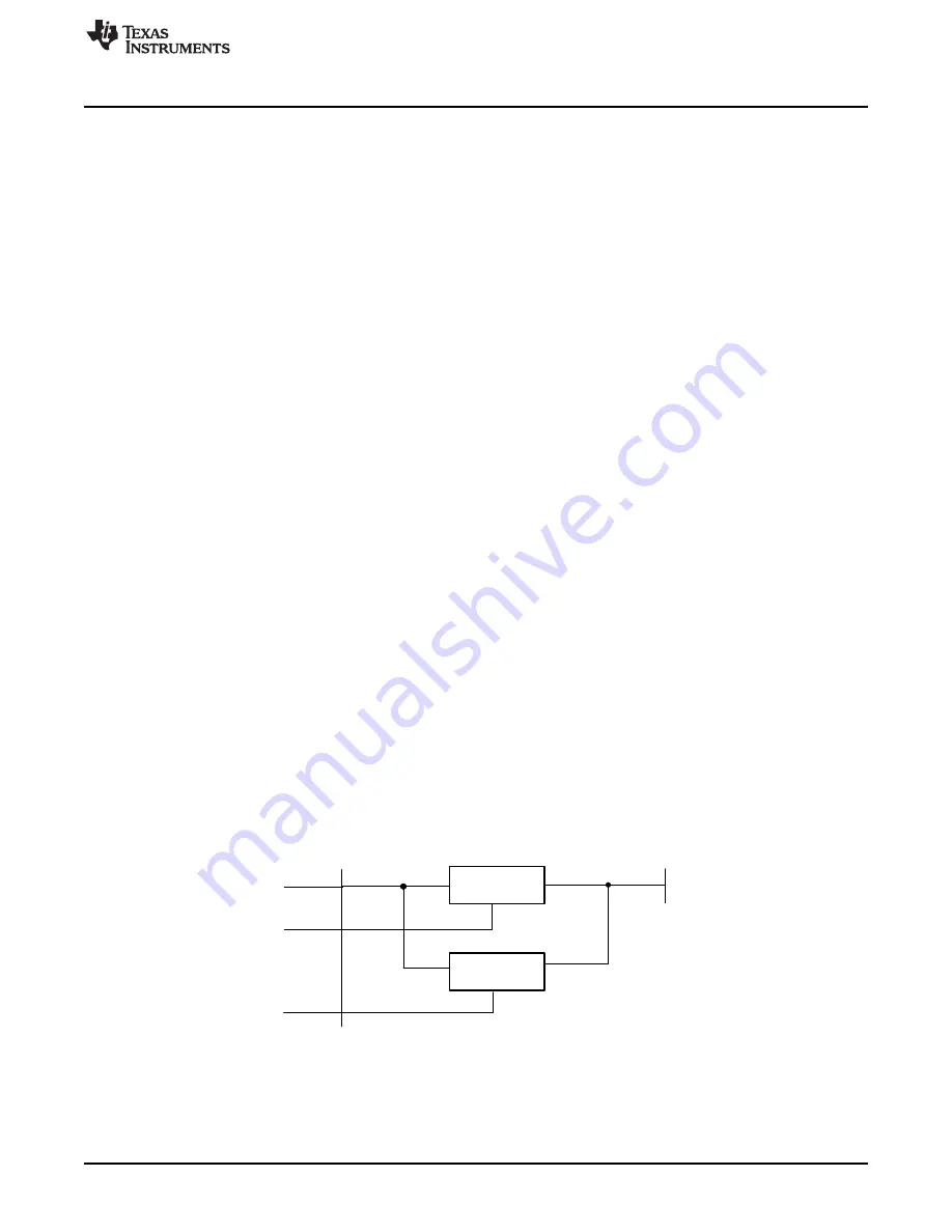
The MSP432E4 microcontroller contains two identical ADC modules. These two modules, ADC0 and
ADC1, share the same 24 analog input channels. Each ADC module operates independently and can
therefore execute different sample sequences, sample any of the analog input channels at any time, and
generate different interrupts and triggers.
shows how the two modules are connected to
analog inputs and the system bus.
Figure 10-1. Implementation of Two ADC Blocks
provides details on the internal configuration of the ADC controls and data registers.


