Rev. 1.0, 02/00, page 905 of 1141
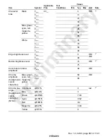
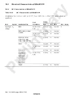
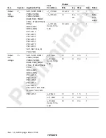
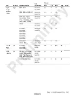
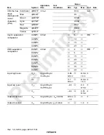
Values
Item
Symbol
Applicable Pins
Test
Conditions
Min
Typ
Max
Unit
Notes
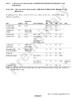
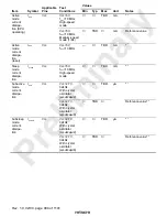
Vcc=2.7V,
32kHz
With crystal
oscillator
TBD
µ
A
*
3
Watch
mode
current
dissipa-
tion
I
WATCH
Vcc
Vcc=5.0V,
32kHz
With crystal
oscillator
TBD
µ
A
Reference
value
*
3
Standby
mode
current
dissipa-
tion
I
STBY
Vcc
X1=V
CL
, 32kHz
Without crystal
oscillator
5
µ
A
*
3
RAM data
retaining
voltage in
standby
mode
V
STBY
2.0
V
Notes: 1. Do not open the AVcc and AVss pin even when the A/D converter is not in use.
2. Current value when the relevant bit of the pull-up MOS select register (PUR1 to PUR3)
is set to 1.
3. The current on the pull-up MOS or the output buffer excluded.
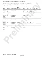
Table 30.13 Pin Status at Current Dissipation Measurement
Mode
5(6
5(6
5(6
5(6
pin
Internal State
Pin
Oscillator Pin
Active mode
High-speed, medium-
speed
Vcc
Operating
Vcc
Sleep mode
High-speed, medium-
speed
Vcc
Only CPU and
servo circuits
halted
Vcc
Reset
Vss
Reset
Vcc
Standby mode
Vcc
All circuits halted
Vcc
Main clock:
Crystal oscillator
Sub clock:
X1 pin = V
CL
Subactive mode
Vcc
CPU and timer A
operating
Vcc
Subsleep mode
Vcc
Timer A operating
Vcc
Watch mode
Vcc
Timer A operating
Vcc
Main clock:
Crystal oscillator
Sub clock:
Crystal oscillator


