Rev. 1.0, 02/00, page 679 of 1141
26.12.2
Pin Configuration
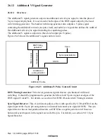
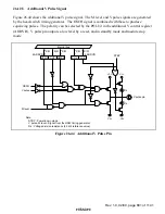
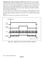
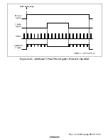
Table 26.16 summarizes the pin configuration of the additional V signal.
Table 26.16 Pin Configuration
Name
Abbrev.
I/O
Function
Additional V pulse pin
Vpulse
Output
Output of additional V signal synchronized to
video FF
26.12.3
Register Configuration
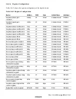
Table 26.17 summarizes the register that controls the additional V signal.
Table 26.17 Register Configuration
Name
Abbrev.
R/W
Size
Initial Value
Address
Additional V control register
ADDVR
R/W
Byte
H'E0
H'D06F
26.12.4
Register Description
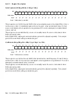
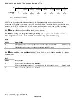
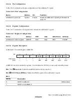
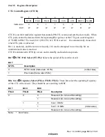
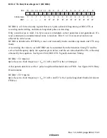
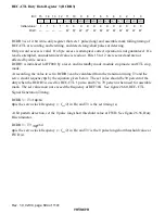
Additional V Control Register (ADDVR)
0
0
1
0
R/W
2
0
R/W
3
0
4
0
R/W
5
1
6
7
—
—
—
—
—
—
R/W
R/W
HMSK
HiZ
CUT
VPOM
POL
1
1
Bit :
Initial value :
R/W :
ADDVR is an 8-bit read/write register. It is initialized to H'E0 by a reset, and in standby mode.
Bits 7 to 5
Reserved: Cannot be modified and are always read as 1.
Bit 4
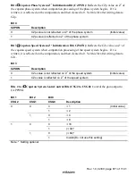
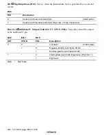
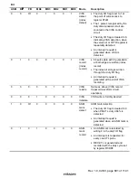
OSCH Mask (HMSK): Masks the OSCH signal in the additional V signal.
Bit 4
HMSK
Description
0
OSCH is added in
(Initial value)
1
OSCH is not added in

