


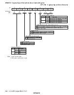

Rev. 1.0, 02/00, page 1004 of 1141
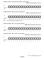
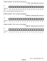
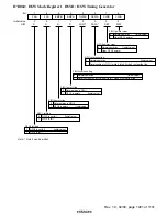
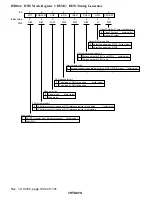
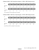
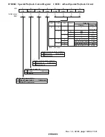
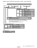
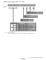
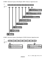
H'D064 to H'D065: FIFO Output Pattern Register 1 FPDRA: HSW Timing Generator
8
*
9
*
W
10
*
W
11
*
12
*
W
*
W
13
14
*
15
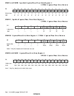
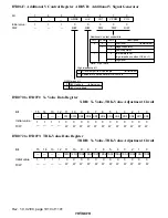
NarrowFFA
VFFA
AFFA
VpulseA
MlevelA
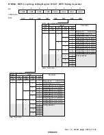
1
W
MlevelA bit
Used for generating an additional
V signal. For details, refer to section
26.12, Additional V Signal Generator.
VpulseA bit
Used for generating an additional
V signal. For details, refer to section
26.12, Additional V Signal Generator.
AudioFFA bit
Controls the audio head.
VideoFFA bit
Controls the video head.
NarrowFFA bit
Controls the narrow video head.
A/D Trigger A bit
Indicates a hardware trigger signal for the A/D converter.
Reserved
Cannot be read or modified
S-TRIGA bit
Indicates a signal that generates an interrupt.
When the STRIGA is selected by the ISEL,
modifying this bit from 0 to 1 generates an interrupt.
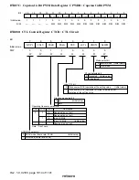
MlevelA bit
Used for generating an additional
V signal. For details, refer to section
26.12, Additional V Signal Generator.
VpulseA bit
Used for generating an additional
V signal. For details, refer to section
26.12, Additional V Signal Generator.
AudioFFA bit
Controls the audio head.
VideoFFA bit
Controls the video head.
NarrowFFA bit
Controls the narrow video head.
A/D Trigger A bi
Indicates a hardware trigger signal for the A/D converter.
Reserved
Cannot be read or modified
S-TRIGA bit
Indicates a signal that generates an interrupt.
When the STRIGA is selected by the ISEL,
modifying this bit from 0 to 1 generates an interrupt.
W
W
ADTRGA
STRIGA
Bit
Initial value
R/W
Bit
Initial value
R/W
0
*
1
*
W
2
*
W
3
*
4
*
W
*
W
5
6
*
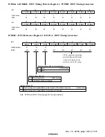
7
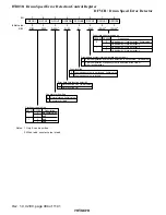
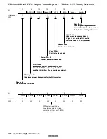
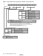
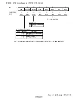
PPGA4
PPGA3
PPGA2
PPGA1
PPGA0
*
W
PPGA7
W
W
W
PPGA6
PPGA5
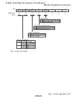
:
:
:
:
:
:
PPG output signal A bits
Used for outputting a timing
control signal from port 7 (PPG).