Rev. 1.0, 02/00, page 185 of 1141
Section 10 I/O Port
10.1
Overview
10.1.1
Port Functions
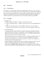
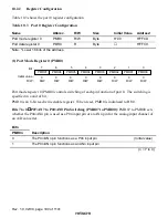
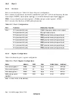
This LSI has seven 8-bit I/O ports (including one CMOS high-current port), and one 8-bit input
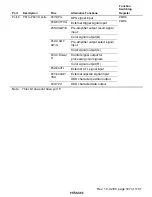
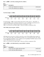
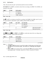
port. Table 10.1 shows the functions of each port. Each I/O part a port control register (PCR) that
controls an input and output and a port data register (PDR) for storing output data. The input and
output can be controlled in a unit of bit. The pin whose peripheral function is used both as an
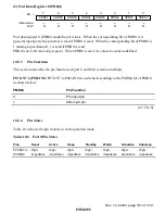
alternative function can set the pin function in a unit of bit by a port mode register (PMR).
10.1.2
Port Input
•
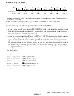
Reading a Port
When a general port of PCR = 0 (input) is read, the pin level is read.
When a general port of PCR = 1 (output) is read, the value of the corresponding PDR bit is
read.
When the pins (excluding AN7 to AN0 and RPB7 to RP0 pins) set to the peripheral
function are read, the results are as given in items (1) and (2) according to the PCR value.
•
Processing Input Pins
The general input port or general I/O port is gated by read signals. Unused pins can be left
open if they are not read. However, if an open pin is read, a feedthrough current may apply
during the read period according to an intermediate level. The read period is about one-state.
Relevant ports: P0, P1, P2, P3, P4, P5, P6, P7, and P8
When an alternative pin is set to an alternative function other than the general I/O, always set
the pin level to a high or low level. If the pin is left open, a feedthrough current applies
according to an intermediate level, which adversely affects reliability, causes malfunctions,
and in the worst case may damage the pin.
Because the PMR is not initialized in low power consumption mode, pay attention to the pin
input level after the mode has been shifted to the low power consumption mode.
Relevant pins:
,&
,
,54
3
to
,54
8
, SCK1, SI1, SDA1, SCL1, SDA0, SCL0, SYNCI, FTIA,
FTIB, FTIC, FTID, RPTRG, TMBI,
$'75*
, EXCTL, COMP, DPG, EXCAP, and EXTTRG


