Rev. 1.0, 02/00, page 409 of 1141
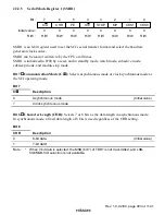
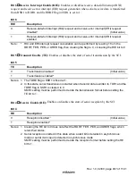
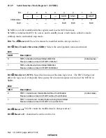
Bits 1 and 0
Clock Enable 1 and 0 (CKE1, CKE0): These bits are used to select the SCI clock
source and enable or disable clock output from the SCK pin. The combination of the CKE1 and
CKE0 bits determines whether the SCK pin functions as an I/O port, the serial clock output pin, or
the serial clock input pin.
The setting of the CKE0 bit, however, is only valid for internal clock operation (CKE1 = 0) in
asynchronous mode. The CKE0 bit setting is invalid in synchronous mode, and in the case of
external clock operation (CKE1 = 1). Note that the SCI's operating mode must be decided using
SMR1 before setting the CKE1 and CKE0 bits.
For details of clock source selection, see table 22.9 in section 22.3, Operation.
Bit 1
Bit 0
CKE1
CKE0
Description
Asynchronous mode
Internal clock/SCK pin functions as I/O port
*1
0
Clock synchronous
mode
Internal clock/SCK pin functions as serial
clock output
*1
Asynchronous mode
Internal clock/SCK pin functions as clock
output
*2
0
1
Clock synchronous
mode
Internal clock/SCK pin functions as serial
clock output
Asynchronous mode
External clock/SCK pin functions as clock
input
*3
0
Clock synchronous
mode
External clock/SCK pin functions as serial
clock input
Asynchronous mode
External clock/SCK pin functions as clock
input
*3
1
1
Clock synchronous
mode
External clock/SCK pin functions as serial
clock input
Notes: 1. Initial value.
2. Outputs a clock of the same frequency as the bit rate.
3. Inputs a clock with a frequency 16 times the bit rate.

