Rev. 1.0, 02/00, page 1021 of 1141
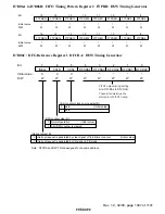
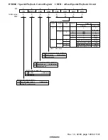
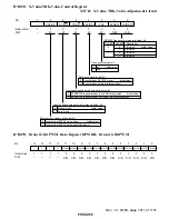
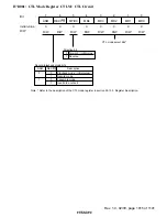
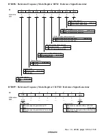
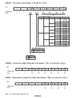
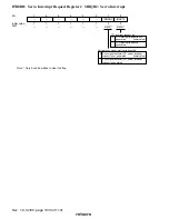
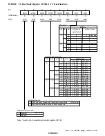
H'D09A: DVCFG Control Register CDVC: Frequency Divider
0
0
1
0
W
2
0
W
3
4
0
W
5
1
6
1
7
W
R
CMK
CMN
W
DVTRG
0
R/W*
MCGin
CRF
CPS1
CPS0
0
Note: * Only 0 can be written
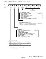
Mask CFG flag
0 CFG normal operation
(Initial value)
1 DVCFG is detected while mask is set (race detection)
CFG mask status bit
0 Mask is released by capstan mask timer
1 Mask is set by capstan mask timer
(Initial value)
CFG mask select bit
0 Capstan mask timing function ON
(Initial value)
1 Capstan mask timing function OFF
PB (ASM)-to-REC transition timing sync ON/OFF select bit
0 PB (ASM)-to-REC transition timing sync ON
(Initial value)
1 PB (ASM)-to-REC transition timing sync OFF
CFG frequency division edge select bit
0 Execute frequency division operation at CFG rising edge
(Initial value)
1 Execute frequency division operation at CFG rising
CFG mask timer clock select bit
CPS1 CPS0 Description
0 0
φ
s/1024
(Initial value)
1
φ
s/512
1 0
φ
s/256
1
φ
s/128
—
—
Bit
Initial value
R/W
:
:
:
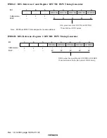
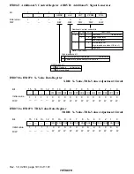
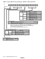
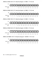
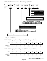
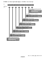
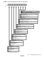
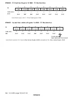
H'D09B: CFG Frequency Division Register 1 CDIVR1: Frequency Divider
0
0
1
0
W
2
0
W
3
4
0
W
5
0
6
7
W
W
CDV15
CDV14
0
W
CDV16
0
W
CDV13
CDV12
CDV11
CDV10
1
Bit :
Initial value :
R/W :
—
—
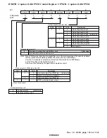
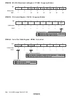
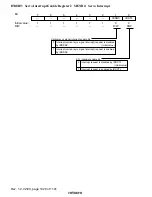
H'D09C: CFG Frequency Division Register 2 CDIVR2: Frequency Divider
0
0
1
0
W
2
0
W
3
4
0
W
5
0
6
7
W
W
CDV25
CDV24
0
W
CDV26
0
W
CDV23
CDV22
CDV21
CDV20
1
Bit :
Initial value :
R/W :
—
—

