Rev. 1.0, 02/00, page 630 of 1141
26.7.2
Block Diagram
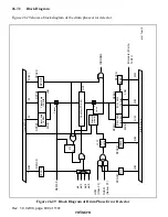
Figure 26.29 shows a block diagram of the drum phase error detector.
R/W
R/W
R/W
R/W
R/W
R/W
REF30P
HSW
(Video FF)
NHSW
(Narrow FF)
DPGCR
DPGCR
DPGCR
DFUCR
DPGCR
DPPR1
DPPR2
R/(W)
S
R
F/F
Q
W
W
Internal bus
Internal bus
OVF
LSB
MSB
DPER1
DPER2
LSB
MSB
DPOVF
DFEPS
HSWES
N/V
Latch
Preset
Error data (20 bits)
To DFU
Edge
detector
Sequence
controller
↑
,
↓
Error data
(16 bits)
Error data
(4 bits)
Preset data
(16 bits)
Preset data
(4 bits)
Counter (20 bits)
IRRDRM3
DPCS1,0
φ
s
φ
s/2
φ
s/4
φ
s/8
φ
s = fosc/2
Figure 26.29 Block Diagram of Drum Phase Error Detector

