Rev. 1.0, 02/00, page 452 of 1141
•
Break Detection and Processing
When framing error (FER) detection is performed, a break can be detected by reading the SI1
pin value directly. In a break, the input from the SI1 pin becomes all 0s, and so the FER flag is
set, and the parity error flag (PER) may also be set.
Note that, since the SCI continues the receive operation after receiving a break, even if the
FER flag is cleared to 0, it will be set to 1 again.
•
Sending a Break
The SO1 pin has a dual function as an I/O port whose direction (input or output) is determined
by DR and DDR. This can be used to send a break.
Between serial transmission initialization and setting of the TE bit to 1, the mark state is
replaced by the value of PDR (the pin does not function as the SO1 pin until the TE bit is set to
1). Consequently, PCR and PDR for the port corresponding to the SO1 pin are first set to 1.
To send a break during serial transmission, first clear PDR to 0, then clear the TE bit to 0.
When the TE bit is cleared to 0, the transmitter is initialized regardless of the current
transmission state, the SO1 pin becomes an I/O port, and 0 is output from the SO1 pin.
•
Receive Error Flags and Transmit Operations (Clocked Synchronous Mode Only)
Transmission cannot be started when a receive error flag (ORER, PER, or FER) is set to 1,
even if the TDRE flag is cleared to 0. Be sure to clear the receive error flags to 0 before
starting transmission.
Note also that receive error flags cannot be cleared to 0 even if the RE bit is cleared to 0.
•
Receive Data Sampling Timing and Reception Margin in Asynchronous Mode
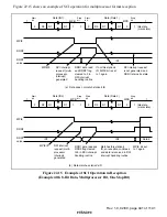
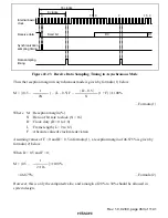
In asynchronous mode, the SCI operates on a basic clock with a frequency of 16 times the
transfer rate.
In reception, the SCI samples the falling edge of the start bit using the basic clock, and
performs internal synchronization. Receive data is latched internally at the rising edge of the
8th pulse of the basic clock. This is illustrated in figure 22.23.

