Rev. 1.0, 02/00, page 734 of 1141
26.15.2
Block Diagram
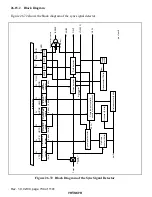
Figure 26.72 shows the block diagram of the sync signal detector.
W
H threshold
register
W
V threshold
register
(6 bits)
(4 bits)
HTR
VTR
W
W
H complement
start time register
Complementary
H pulse width
register
(8 bits)
(4 bits)
HPWR
HRTR
W
W
(6 bits)
(8 bits)
NDR
R/W
R/W
R/(W)
R
NOIS
H counter (8 bits)
Noise detector
Complement control &
nozzle mask control circuit
Up/Down
counter (6 bits)
SEPH
Selection of
polarity
Noise detection
window
Noise detection interrupt
VD interrupt
Csync
Sync signal detector
H reload counter (8 bits)
Field detector
Noise counter (10 bits)
Toggle
circuit
Clear
FLD
SYCT
VD(SEPV)
FIELD
NOISE
IRRSNC
OSCH
NIS/VD
SYNCR
NWR
Internal bus
φ
s = fosc/2
φ
s/2
Noise detection
window register
Noise
detection register
Figure 26.72 Block Diagram of the Sync Signal Detector


