Rev. 1.0, 02/00, page 719 of 1141
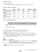
DVCTL Control Register (CTVC)
0
*
1
*
R
2
*
R
3
4
5
6
7
R
CFG
HSW
0
W
0
W
CEX
CEG
CTL
1
1
1
Bit :
Initial value :
R/W :
CTVC consists of the external input signal selection bits and the flags which show the CFG,
HSW, and CTL levels.
Note:
It has an undetermined value by a reset or in stand-by mode.
Bit 7
DVCTL Signal Generation Selection Bit (CEX): Selects which of the PB-CTL signal or
the external input signal is used to generate the DVCTL signal.
Bit 7
CEX
Description
0
Generates DVCTL signal with PB-CTL signal
(Initial value)
1
Generates DVCTL signal with external input signal
Bit 6
External Sync Signal Edge Selection Bit (CEG): Selects the edge of the external signal
at which the frequency division is made when the external signal was selected to generate DVCTL
signal.
Bit 6
CEG
Description
0
Rising edge
(Initial value)
1
Falling edge
Bits 5 to 3
Reserved: Cannot be modified and are always read as 1.
Bit 2
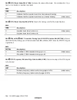
CFG Flag (CFG): Shows the CFG level.
Bit 2
CFG
Description
0
CFG is at low level
(Initial value)
1
CFG is at high level

