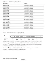
Rev. 1.0, 02/00, page 131 of 1141
7.3
Flash Memory Register Descriptions
7.3.1
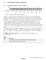
Flash Memory Control Register 1 (FLMCR1)
7
FWE
—*
R
6
SWE1
0
R/W
5
ESU1
0
R/W
4
PSU1
0
R/W
3
EV1
0
R/W
0
P1
0
R/W
2
PV1
0
R/W
1
E1
0
R/W
Bit
Initial value
R/W
:
:
:
Note: * Determined by the state of the FWE pin.
FLMCR1 is an 8-bit register used for flash memory operating mode control. With addresses
H'00000 to H'3FFFF, program-verify mode or erase-verify mode is entered by setting SWE to 1
when FWE = 1, then setting the PV1 bit and EV1 bit. Program mode is entered by setting SWE1
when FWE = 1, then setting the SWE1 bit and PSU1, and finally setting the P1 bit. With
addresses H'00000 to H'3FFFF, erase mode is entered by setting SWE1 when FWE = 1, then
setting the ESU1 bit, and finally setting the E1 bit. FLMCR1 is initialized by a reset, and in
standby mode. Its initial value is H'80 when a high level is input to the FWE pin, and H'00 when a
low level is input. When on-chip flash memory is disabled, a read will return H'00, and writes are
invalid.
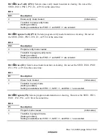
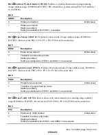
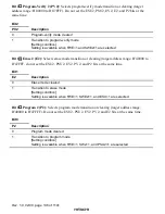
Writes to the SWE1 bit in FLMCR1 are enabled only when FWE = 1; writes to the ESU1, PSU1,
EV1 and PV1 bits only when FWE = 1 and SWE1 = 1; writes to the E1 bit only when FWE = 1,
SWE1 = 1, and ESU1 = 1; and writes to the P1 bit only when FWE = 1, SWE1 = 1, and PSU1 = 1.
Bit 7
Flash Write Enable (FWE): Sets hardware protection against flash memory
programming/erasing.
Bit 7
FWE
Description
0
When a low level is input to the FWE pin (hardware-protected state)
1
When a high level is input to the FWE pin


