Rev. 1.0, 02/00, page 658 of 1141
26.10.3
Register Description
Register Configuration
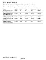
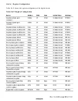
Table 26.13 shows the register configuration of X-value correction and tracking correction
circuits.
Table 26.13 Register Configuration
Name
Abbrev.
R/W
Size
Initial Value
Address
X-value and TRK-value
control register
XTCR
R/W
Byte
H'80
H'D074
X-value data register
XDR
W
Word
H'F000
H'D070
TRK-value data register
TRDR
W
Word
H'F000
H'D072
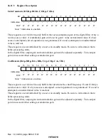
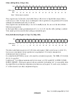
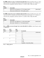
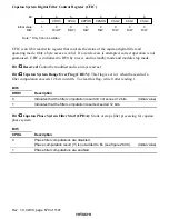
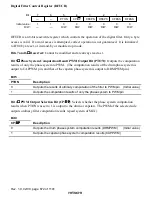
X-Value and TRK-Value Control Register (XTCR)
0
0
1
0
R*/W
2
0
W
3
0
4
0
W
5
0
6
0
7
—
—
R*/W
W
W
AT/MU
W
CAPRF
TRK/X
EXC/REF
XCS
DVREF1
DVREF0
1
Bit :
Initial value :
R/W :
XTCR is an 8-bit register to determine the X-value and TRK-value correction circuits. Bits 6 to 2
are write-only bits. No read is valid. If a read is attempted, an undetermined value is read out.
Bits 1 and 0 are read/write bits. Only a byte access is valid for XTCR. If a word access is
attempted, correct operation is not guaranteed.
It is initialized to H'80 by a reset, or in stand-by or module stop mode.
Bit 7
Reserved: Cannot be modified and is always read as 1.
Bit 6
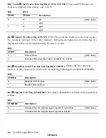
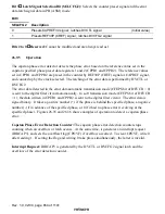
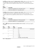
External Sync Signal Edge Selection Bit (CAPRF): Selects the EXCAP edge when a
selection is made to generate external sync signals.
Bit 6
CAPRF
Description
0
Signal generated at the rising edge of EXCAP.
(Initial value)
1
Signal generated at both edges of EXCAP.

