Rev. 1.0, 02/00, page 985 of 1141
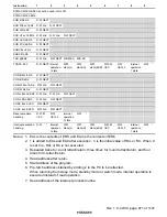
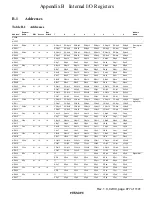
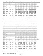
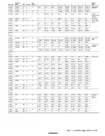
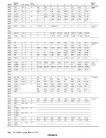
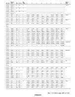
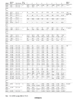
Address*
1
Register
Name
R/W
Access
Bus
Width
7
6
5
4
3
2
1
0
Module
Name
H'FFF8
FLMCR1
R/W
8
8
FWE
SWE1
ESU1
PSU1
EV1
PV1
E1
P1
H'FFF9
FLMCR2
R/W
8
8
FLER
SWE2
ESU2
PSU2
EV2
PV2
E2
P2
H'FFFA
EBR1
R/W
8
8
EB7
EB6
EB5
EB4
EB3
EB2
EB1
EB0
H'FFFB
EBR2
R/W
8
8
EB15
EB14
EB13
EB12
EB11
EB10
EB9
EB8
Flash memory
H'FFFC
H'FFFD
H'FFFE
H'FFFF
Notes:
1.
Lower 16bits of the address.
2.
Assigned to the same address.
3.
Access varies depending on the ICE bit.
4.
OCRA and OCRB address are the same, which can be switched by the OCSR bit in TOCR.
5.
The address is H'FFBC when written to. WTCNT and WTCSR are assigned to the same address. Refer to section 17.2.4, Notes on
Register Access.

