Rev. 1.0, 02/00, page 595 of 1141
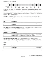
HSW Mode Register 2 (HSM2)
0
0
1
0
R
2
0
R/W
3
0
4
0
R/W
0
R/W
5
6
0
7
EDG
ISEL1
SOFG
OFG
VFF/NFF
0
R/W
FRT
W
R/W
R
FGR2OFF
LOP
Bit :
Initial value :
R/W :
HSM2 is an 8-bit register which confirms and determines the operational state of the HSW timing
generator.
Bit 1 is a read-only bit, and write is disabled. Bit 0 is a write-only bit, and if a read is attempted,
an undetermined value is read out. All the other bits accept both read and write. It is initialized to
H'00 by a reset or in stand-by mode.
Bit 7
Free-run Bit (FRT): Selects whether the matching timing is determined by the DPG
counter and timer, or by the FRC.
Bit 7
FRT
Description
0
5-bit DFG c 16-bit timer counter
(Initial value)
1
16-bit FRC
Bit 6
FRG2 Clear Stop Bit (FGR2OFF): Disables clearing of the counter by the DFG register
2. The FIFO group, including both FIFO1 and FIFO2, is available.
Bit 6
FGR2OFF
Description
0
Enables clearing of the16-bit timer counter by DFG register 2
(Initial value)
1
Disables clearing of the16-bit timer counter by DFG register 2
Bit 5
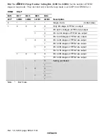
Mode Selection Bit (LOP): Selects the output mode of FIFO. If the loop mode is
selected, LOB3 to LOB0 bits and LOA3 to LOA0 bits become valid. If the LOP bit is modified,
the pointer which counts the writing position of FIFO is cleared. In this case, the last output data
is kept.
Bit 5
LOP
Description
0
Single mode
(Initial value)
1
Loop mode


