Rev. 1.0, 02/00, page 1134 of 1141
3. OSD
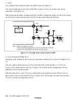
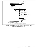
An example of the external circuit for the OSD is shown in figure E.5.
The circuit configuration and values for the filter section will vary according to the wiring
capacitance, impedance, etc.
When designing the board, an appropriate filter should be configured, taking account of the wiring
load. Noise prevention measures also need to be taken when designing the board.
Clamp
(=1.4Vtyp)
Note: Reference values are shown.
The board floating capacitance and wiring resistance must also
be taken into consideration in determining the values.
C.Vin1
C.Vout
4.7
µ
F
470
µ
F
+
68
Ω
75
Ω
driver
1k
Ω
2.7k
Ω
470k
Ω
120
Ω
5pF
Figure E.5 Example of External Circuit for OSD
4. Sync Separator and Data Slicer
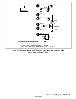
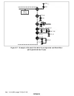
Examples of the external circuits for the sync separator and data slicer are shown in figures E.6 to
E.8.
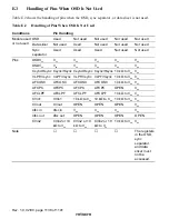
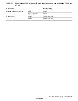
The sync signal separation sources can be selected from the following three: (1) CVin2, (2)
Csync, and (3) separate Hsync and Vsync signals. The external circuit configuration will vary
depending on the separation source.
When the data slicer is used, CVin2 is recommended as the separation source. When Csync or
Hsync and Vsync are selected as the source, connect to CVin2 the same external circuit as when
CVin2 is selected as the separation source.

