Rev. 1.0, 02/00, page 1118 of 1141
Pin States
Pin Names
Circuit Diagram
At Reset
Sleep
Mode
Power-Down
Modes Other
Than Sleep
Mode
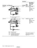
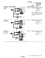
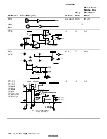
P21/SO1
PUR21·
SO1
PDR21
TXE
PCR21
RD
TXE: Output control signal determined
by SCR and SMR
Hi-Z
Retained Pull-up MOS:
OFF
Subactive mode:
Functions
Other modes:
Hi-Z
Retained Pull-up MOS:
OFF
Subactive mode:
Functions
Other modes:
Hi-Z
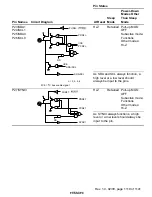
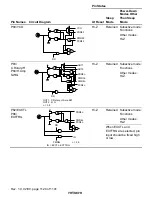
P22/SCK1
PUR22·
SCKO
SCKI
PDR22
CKOE
PCR22
RD
CKIE
SCKO:
Transfer clock output
SCKI:
Transfer clock input
CKOE:
Transfer clock output control signal
determined by SMR and SCR
CKIE:
Transfer clock input control signal
determined by SMR and SCR
Hi-Z
When SCK1 is selected,
pin input should be fixed
high or low.

