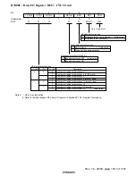
Rev. 1.0, 02/00, page 1007 of 1141
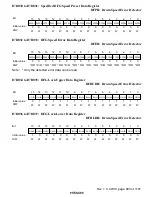
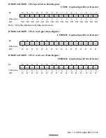
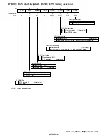
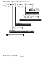
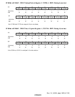
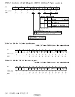
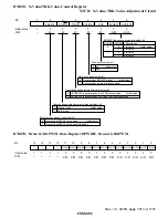
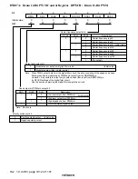
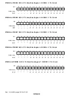
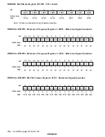
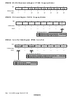
H'D06A to H'D06B: FIFO Timing Pattern Register 2 FTPRB: HSW Timing Generator
8
*
9
*
W
10
*
W
11
*
12
*
W
*
W
13
14
*
15
FTPRB12
FTPRB11
FTPRB10
FTPRB9
FTPRB8
W
W
W
*
W
FTPRB14
FTPRB15
FTPRB13
Bit
Initial value
R/W
:
:
:
8
*
9
*
W
10
*
W
11
*
12
*
W
*
W
13
14
*
15
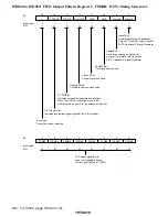
FTPRB12
FTPRB11
FTPRB10
FTPRB9
FTPRB8
W
W
W
*
W
FTPRB14
FTPRB15
FTPRB13
Bit
Initial value
R/W
:
:
:
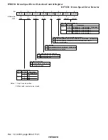
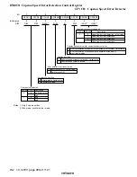
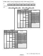
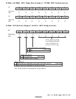
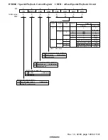
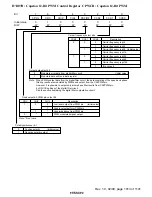
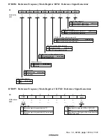
H'D06C: DFG Reference Register 1 DFCRA: HSW Timing Generator
0
*
1
*
W
2
*
W
3
*
4
*
W
0
W
5
6
0
7
DFCRA4
DFCRA3
DFCRA2
DFCRA1
DFCRA0
0
W
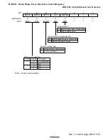
ISEL2
W
W
W
CCLR
CKSL
Interrupt select bit
Note: DFCRA and DFCTR are assigned to the same address.
0 Interrupt request is generated by clear signal of 16-bit timer counter
(Initial value)
1 Interrupt request is generated by VD signal in PB mode
DFG counter clear bit
0 Normal operation (Initial value)
1 5-bit DFG counter is cleared
16-bit counter clock source select bit
0
φ
s/4
(Initial value)
1
φ
s/8
Bit
Initial value
R/W
:
:
:
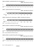
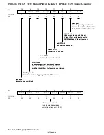
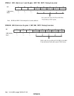
FIFO1 output timing setting
bits (DFCRA4 to DFCRA0)
These bits determine the
start point of FIFO1 timing.

