Rev. 1.0, 02/00, page 62 of 1141
3.2
Register Descriptions
3.2.1
Mode Control Register (MDCR)
0
—*
1
0
2
0
3
0
4
0
5
—
—
—
—
—
0
6
—
0
7
—
—
—
—
—
—
—
—
R
MDS0
0
Bit :
Initial value :
R/W :
Note: *
Determined by MD0 pin
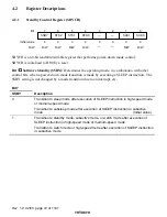
MDCR is an 8-bit read-only register monitors the current operating mode of this LSI.
Bit 7 to 1: Reserved.
These bits cannot be modified and are always read as 0.
Bit 0: Mode Select 0 (MDS0)
This bit indicates the value which reflects the input levels at mode pin (MD0) (the current
operating mode). Bit MDS0 corresponds to MD0 pin. They are read-only bits-they cannot be
written to. The mode pin (MD0) input levels are latched into these bits when MDCR is read.
3.2.2
System Control Register (SYSCR)
0
—
1
1
0
—
2
0
—
3
1
4
0
R/W
5
0
6
—
0
7
—
—
—
—
R
R
INTM1
INTM0
XRST
—
—
0
Bit :
Initial value :
R/W :
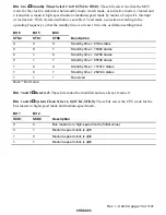
Bits 7 and 6
Reserved: These bits cannot be modified and are always read as 0.

