Rev. 1.0, 02/00, page 1041 of 1141
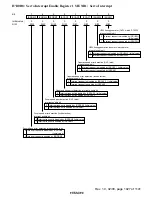
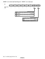
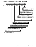
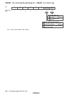
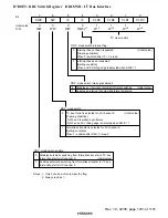
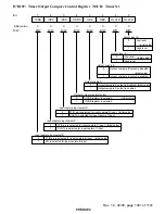
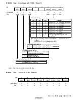
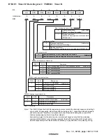
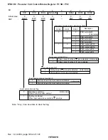
H'D107: Timer Output Compare Control Register TOCR: Timer X1
0
0
1
0
2
0
3
0
4
0
5
0
6
0
7
R/W
R/W
ICSC
0
R/W
ICSB
R/W
OSRS
R/W
ICSD
R/W
OEB
R/W
OEA
OLVLB
R/W
OLVLA
FTIB pin is selected for input capture B input (Initial value)
VD is selected for input capture B input
0
1
Input capture input select B
Low level
(Initial value)
High level
0
1
Output level B
FTIC pin is selected for input capture C input (Initial value)
DVCTL is selected for input capture C input
0
1
Input capture input select C
FTID pin is selected for input capture D input (Initial value)
NHSW is selected for input capture D input
0
1
Input capture input select D
OCRA register is selected
(Initial value)
OCRB register is selected
0
1
Output compare register select
Low level
(Initial value)
High level
0
1
Output level A
Output compare A output is disabled (Initial value)
Output compare A output is enabled
0
1
Output enable A
Initial value :
0
1
Output enable B
Output compare B output is disabled
(Initial value)
Output compare B output is enabled
Bit
R/W
:
:

