Rev. 1.0, 02/00, page 336 of 1141
16.3.5
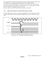
Input Capture Signal Inputting Timing
•
Input Capture Signal Inputting Timing
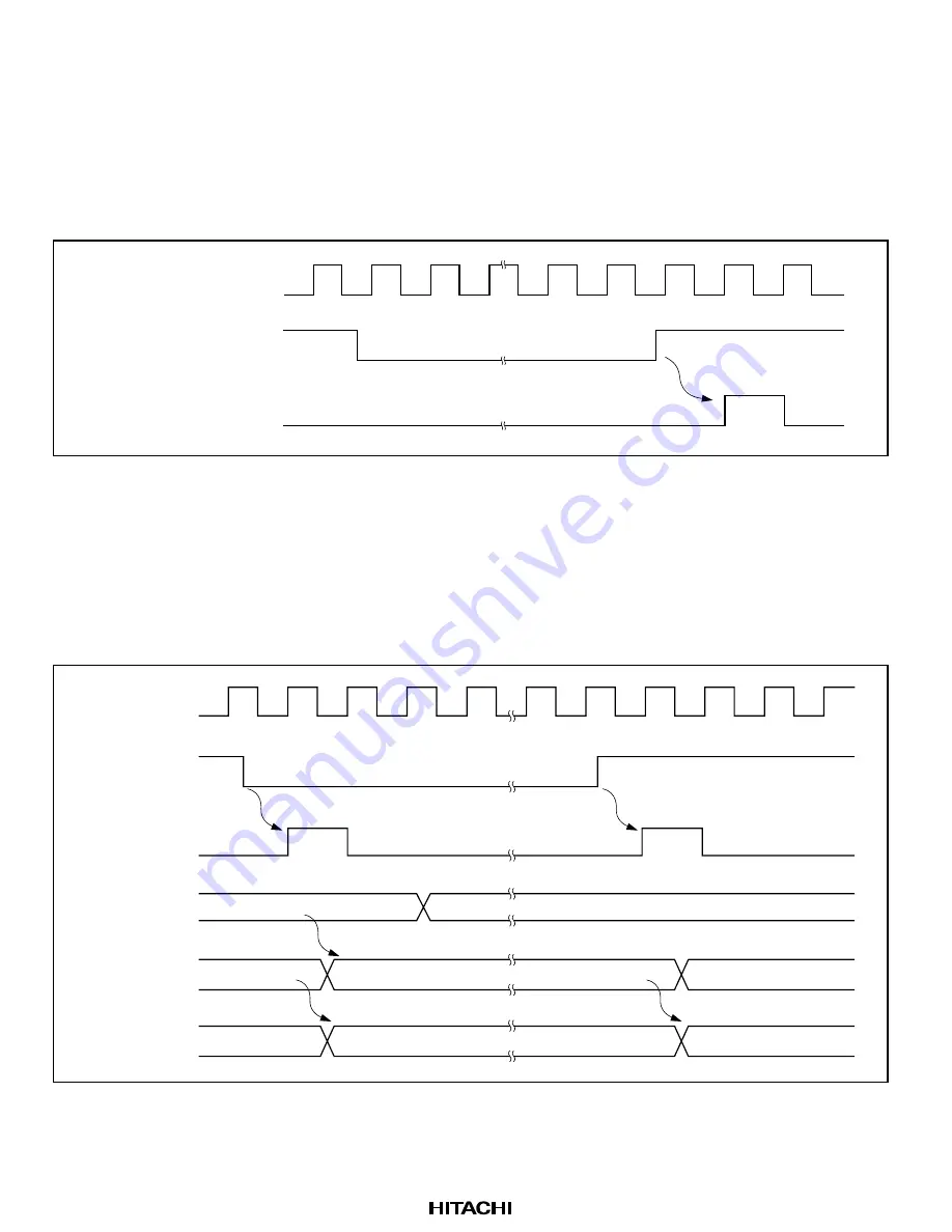
As for the input capture signal inputting, rising or falling edge is selected by settings of the
IEDGA through IEDGD bits of the TCRX.
Figure 16.7 shows the timing chart when the rising edge is selected (IEDGA through IEDGD =
1).
Input capture signal
inputting pin
φ
Input capture signal
Figure 16.7 Input Capture Signal Inputting Timing (under normal state)
•
Input Capture Signal Inputting Timing when Making Buffer Operation
Buffer operation can be made using the ICRA or ICRD as the buffer of the ICRA or ICRB.
Figure 16.8 shows the input capture signal inputting timing chart in case both of the rising and
falling edges are designated (IEDGA = 1 and IEDGC = 0, or IEDGA = 0 and IEDGC = 1),
using the ICRC as the buffer register for the ICRA (BUFEA = 1).
Input capture
signal
FTIA
FRC
ICRA
ICRC
n
n+1
N
M
n
m
M
n
M
N
n
φ
Figure 16.8 Input Capture Signal Inputting Timing Chart Under the Buffer Mode
(under normal state)

