Rev. 1.0, 02/00, page 484 of 1141
Bit 0
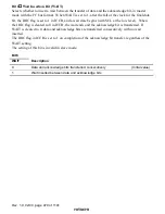
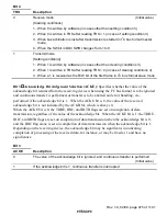
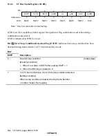
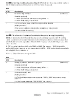
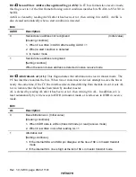
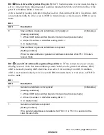
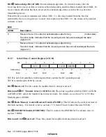
Acknowledge Bit (ACKB): Stores acknowledge data. In transmit mode, after the
receiving device receives data, it returns acknowledge data, and this data is loaded into ACKB. In
receive mode, after data has been received, the acknowledge data set in this bit is sent to the
transmitting device.
When this bit is read, in transmission (when TRS = 1), the value loaded from the bus line
(returned by the receiving device) is read. In reception (when TRS = 0), the value set by internal
software is read.
Bit 0
ACKB
Description
0
Receive mode: 0 is output at acknowledge output timing
(Initial value)
Transmit mode: Indicates that the receiving device has acknowledged the data
(signal is 0)
1
Receive mode: 1 is output at acknowledge output timing
Transmit mode: Indicates that the receiving device has not acknowledged the data
(signal is 1)
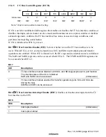
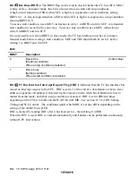
23.2.7
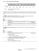
Serial/Timer Control Register (STCR)
7
—
0
—
6
IICX1
0
R/W
5
IICX0
0
R/W
4
—
0
—
3
FLSHE
0
R/W
0
—
0
—
2
OSROME
0
R/W
1
—
0
—
Bit :
Initial value :
R/W :
STCR is an 8-bit readable/writable register that controls the IIC operating mode.
STCR is initialized to H'00 by a reset.
Bit 7
Reserved: This bit cannot be modified and is always read as 0.
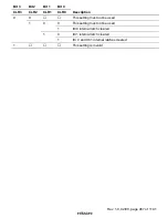
Bits 6 and 5
I
2
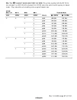
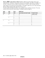
C Transfer Select 1, 0 (IICX1, 0): These bits, together with bits CKS2 to CKS0
in ICMR of IIC, select the transfer rate in master mode. For details, see section 23.2.4, I
2
C Bus
Mode Register (ICMR).
Bit 3
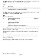
Flash Memory Control Resister Enable (FLSHE): This bit selects the control resister of
the flash memory. For details, refer to section 7.3.5, Serial Timer Control Resister (STCR).
Bit 2
OSD ROM Enable (OSROME): This bit controls the OSD ROM. For details, refer to
section 7, ROM.
Bits 4 and 2 to 0
Reserved: These bits cannot be modified and are always read as 0.

