Rev. 1.0, 02/00, page 328 of 1141
16.2.6
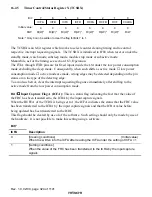
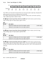
Timer Control Register X (TCRX)
0
0
1
0
2
0
3
0
4
0
5
0
6
0
7
R/W
R/W
IEDGB
0
R/W
IEDGA
R/W
IEDGD
R/W
IEDGC
R/W
BUFEB
R/W
BUFEA
CKS0
R/W
CKS1
Bit :
Initial value :
R/W :
The TCRX is an 8-bit read/write register that selects the input capture signal edge, designates the
buffer operation, and selects the inputting clock for the FRC.
The TCRX is initialized to H'00 when reset or under the standby mode, watch mode, subsleep
mode, module stop mode or subactive mode.
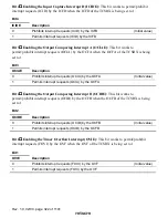
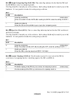
Bit 7
Input Capture Signal Edge Selection A (IEDGA): This bit works to select the rising
edge or falling edge of the input capture signal A (FTIA).
Bit 7
IEDGA
Description
0
Captures the falling edge of the input capture signal A
(Initial value)
1
Captures the rising edge of the input capture signal A
Bit 6
Input Capture Signal Edge Selection B (IEDGB): This bit works to select the rising
edge or falling edge of the input capture signal B (FTIB).
Bit 6
IEDGB
Description
0
Captures the falling edge of the input capture signal B
(Initial value)
1
Captures the rising edge of the input capture signal B
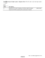
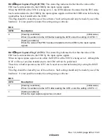
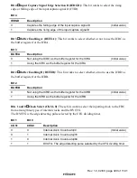
Bit 5
Input Capture Signal Edge Selection C (IEDGC): This bit works to select the rising
edge or falling edge of the input capture signal C (FTIC). However, when the DVCTL has been
selected as the signal for the input capture signal edge selection C, this bit will not influence the
operation.
Bit 5
IEDGC
Description
0
Captures the falling edge of the input capture signal C
(Initial value)
1
Captures the rising edge of the input capture signal C


