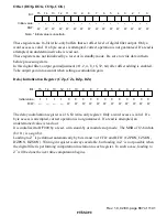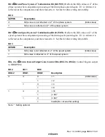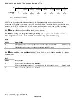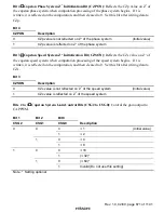
Rev. 1.0, 02/00, page 681 of 1141
26.12.5
Additional V Pulse Signal
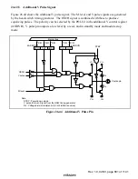
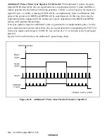
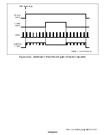
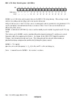
Figure 26.44 shows the additional V pulse signal. The M level and V pulse signals are generated
by the head-switch timing generator. The OSCH signal is combined with these to produce
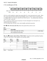
equalizing pulses. The polarity can be selected by the POL bit in the additional V control register
(ADDVR). V pulse pin outputs a low level by a reset, and in standby mode and module stop
mode.
R/W
R/W
á ADDVR
á ADDVR
R/W
Internal bus
R/W
R/W
CUT
VPON
HMSK
POL
HiZ
STBY
V
CC
V
CC
V
SS
V
SS
Rs
Rs
V pulse pin
OSCH
V pulse
M level
Note:
STBY : Power-down mode
V pulse, M level : Signal from the HSW timing generator
Rs : Voltage division resistance (20 k
Ω
: reference value)
Figure 26.44 Additional V Pulse Pin

