Rev. 1.0, 02/00, page 726 of 1141
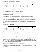
CFG Frequency Division Register 2 (CDIVR2)
0
0
1
0
W
2
0
W
3
4
0
W
5
0
6
7
—
—
W
W
CDV25
CDV24
0
W
CDV26
0
W
CDV23
CDV22
CDV21
CDV20
1
Bit :
Initial value :
R/W :
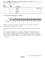
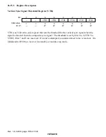
CDIVR2 is an 8-bit write-only register to set the division value. If a read is attempted, an
undetermined value is read out. Bit 7 is reserved.
The frequency division value is written in the reload register and the down counter at the same
time.
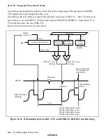
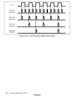
CFG's frequency is divided by N at its rising edge or both edges If the register value was 0, no
division operation is performed, and the DVCFG signal with the same input cycle with CFG is
output. The DVCFG2 signal is sent to the capstan speed error detector and the Timer L.
The DVCFG2 circuit has no mask timer function.
The frequency division counter starts its division operation at the point data was written in
CDIVR2. If synchronization is required for phase matching, for example, do it by writing in
CDIVR2. If the DVTRG bit of the CDVC register is 0, the register synchronizes with the
switching timing from PB (ASM) to REC.
It is initialized to H'80 by a reset or in stand-by mode together with the capstan frequency division
register and the down counter.
DVCFG Mask Period Register (CTMR)
0
1
1
1
W
2
1
W
3
4
1
W
5
1
6
7
—
—
—
—
W
W
CPM5
CPM4
1
W
CPM3
CPM2
CPM1
CPM0
1
1
Bit :
Initial value :
R/W :
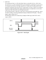
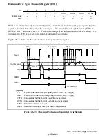
CTMR is an 8-bit write-only register. If a read is attempted, an undetermined value is read out.
CTMR is a reload register for the mask timer (down counter). Set in it the mask period of CFG.
The mask period is determined by the clock specified by the bits 1 and 0 of CDVC and the set
value (N - 1). If data is written in CTMR, it is written also in the mask timer at the same time.
It is initialized to H'FF by a reset, or in stand-by or module stop mode.
Mask period = N
×
clock cycle

