COPYRIGHT © 1999 CANON INC. CANON imageRUNNER 400/330 REV.0 JAN. 1999 PRINTED IN JAPAN (IMPRIME AU JAPON)
4-3
CHAPTER 4 IMAGE FORMATION SYSTEM
II. ANALOG IMAGE PROCESSING
A. Outline
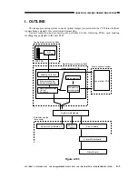
The CCD PCB has the following functions:
Driving the CCD.
Performs A/D conversion of CCD output signals (analog)
Performs AE processing (ABC processing)
B. CCD
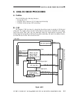
The machine's CCD line sensor is a single-line linear image sensor consisting of 75000-pixel
photocells. The signals photo-converted by the light-receiving unit are transferred to the analog
signal processing block (odd- and even-numbered pixels are communicated separately). The
analog signal processing block combines the signals representing odd- and even-numbered pixels,
and sends the result to the A/D conversion block.
Figure 4-200
CCD
Analog signal processing block
Shading correction data
A/D conversion
AE processing
(ABC processing)
•
Offset correction
•
Gain correction
•
Pixel synthesis
•
Shading correction
Reference voltage
generation
Reference voltage
generation
Odd-numbered
pixels
Even-numbered
pixels
Analog image signal
Digital image signal
Digital image signal
AE processing OFF signal
ABC-TBL signal
CCD PCB
Clock pulse generation
8
8
J303
J301
J706
J301
J706
J301
J706
J301
J706
J705
Line memory
Image processor PCB


