COPYRIGHT © 1999 CANON INC. CANON imageRUNNER 400/330 REV.0 JAN. 1999 PRINTED IN JAPAN (IMPRIME AU JAPON)
4-1
CHAPTER 4 IMAGE FORMATION SYSTEM
I. OUTLINE
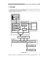
The image processing system converts optical images projected onto the CCD into electrical
signals (image signals) for correction and processing.
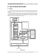
Various correction and processing are performed in the following PCBs, each sending
resulting image signals to the next PCB.
Figure 4-100
CCE PCB
Extension boards
(accessory)
Image processor PCB
Laser driver PCB
Laser exposure system
CCD
A-D
conversion
Shading correction
Binary processing
Screen processing
Resolution conversion
(for fax)
Smoothing
Super G3 FAX Board-F1
PBL I/F Board
Printer Motherboard
Printer Board
SCSI I/F
board
System motherboard
Analog image processing block
Digital image processing block
Compression/
decompression
Image memory

