COPYRIGHT © 1999 CANON INC. CANON imageRUNNER 400/330 REV.0 JAN. 1999 PRINTED IN JAPAN (IMPRIME AU JAPON)
5-5
CHAPTER 5 LASER EXPOSURE SYSTEM
III. LASER DRIVER PCB
A. Outline
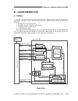
Figure 5-300 shows the laser driver PCB, which drives the laser semiconductor using control
signals and the image signals from the image processor PCB. The circuit has the following
functions:
1. Driving the laser semiconductor
2. Stabilizing the laser intensity (APC control)
3. Switching laser activation mode
4. Switching laser output
The image signals from the image processor are written in the line memory in conjunction with
the sync signals generated for internal use on the laser driver PCB. The laser drive signals are
generated based on these image signals to drive the laser semiconductor.
Figure 5-300
5V
Clock signal
generation for
synchronization
BD detection
PCB
Laser drive
signal
generation
Laser power control
Laser power signal
Laser drive control
APC control
Laser driver PCB
Q504
Q506
Q507
Q509
Q508
Horizontal sync clock
signal
Image signal
Laser semiconductor
Sample voltage
Write enable signal (VDR)
Laser activation mode switch signal
(SDATX: serial data)
Line memory
Image signal
D501
PD
Laser activation enable
signal (LDE)
J717B
J717A
J717B
J500B
Laser output switch signal
(SDATX: serial data)
J717B
J500B
J717B
J500B
J717B
J500B
8
J500B
J500A
Image processor PCB
Target voltage
Laser drive signal

