Rev. 1.0, 02/00, page 885 of 1141
30.2.2
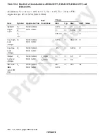
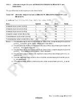
Allowable Output Currents of HD6432199, HD6432198, HD6432197, and
HD6432196
The specifications for the digital pins are shown below.
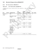
Table 30.5
Allowable Output Currents of HD6432199, HD6432198, HD6432197, and
HD6432196
(Conditions: Vcc = 2.5 V to 5.5 V, Vss = 0.0 V, Ta = –20 to +75
°
C)
Item
Symbol
Value
Unit
Notes
Allowable input current (to chip)
I
O
2
mA
1
Allowable input current (to chip)
I
O
22
mA
2
Allowable input current (to chip)
I
O
10
mA
3
Allowable output current (from chip)
−
I
O
2
mA
4
Total allowable input current (to chip)
Σ
I
O
80
mA
5
Total allowable output current (from chip)
−Σ
I
O
50
mA
6
Notes: 1. The allowable input current is the maximum value of the current flowing from each I/O
pin to V
SS
(except for port 6, SCL0, SDA0, SCL1 and SDA1).
2. The allowable input current is the maximum value of the current flowing from each I/O
pin to V
SS
. This applies to port 6.
3. The allowable input current is the maximum value of the current flowing from each I/O
pin to V
SS
. This applies to SCL0, SDA0, SCL1 and SDA1.
4. The allowable output current is the maximum value of the current flowing from V
CC
to
each I/O pin.
5. The total allowable input current is the sum of the currents flowing from all I/O pins to
V
SS
simultaneously.
6. The total allowable output current is the sum of the currents flowing from V
CC
to all I/O
pins.

