Rev. 1.0, 02/00, page 855 of 1141
29.6
Other Settings
29.6.1
TV Format
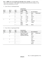
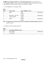
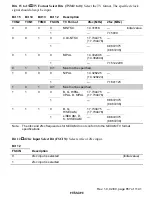
The OSD supports M/NTSC, 4.43-NTSC, M/PAL, N/PAL, B, G, H/PAL, I/PAL, D, K/PAL, and
SECAM formats. See table 29.3, TV Formats and Display Modes.
29.6.2
Display Data RAM Control
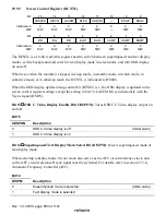
The OSD display data RAM consists of master RAM and slave RAM. The master RAM can be
read and written by the CPU; the slave RAM is accessed by the OSD.
The data written to master RAM is transferred to slave RAM to switch the OSD display.
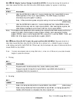
The DTMV bit can be used to switch between timing the transfer of data to occur when the
LDREQ bit is set to 1, or to occur synchronously with the Vsync signal after LDREQ is set to 1.
For details, refer to section 29.6.6, OSD Format Register (DFORM).
29.6.3
Timing of OSD Display Updates Using Register Rewriting
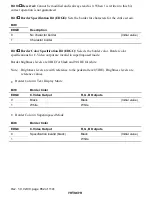
It is possible to switch the timing of OSD display updates to occur simultaneously with register
rewrites, or to occur synchronously with the Vsync signal (OSDV) after a register rewrite. For
details, refer to section 29.6.6, OSD Format Register (DFORM).
29.6.4
4fsc/2fsc
For a 4fsc/2fsc signal, either an external clock signal is input, or a crystal oscillator can be
connected. If an external clock signal is input, the signal must be amplified using a dedicated
amplifier circuit; this is set using the register.
Either 4fsc or 2fsc input can be selected.
If a 2fsc signal is input, some colors cannot be displayed. For details, see table 29.7, OSD Display
Colors for 2fsc Signal Input.
29.6.5
OSDV Interrupts
Interrupts triggered by the Vsync signal input to the OSD (OSDV interrupts) can be generated. In
superimposed mode, interrupts are triggered by the external Vsync signal, and in text display
mode, they are triggered by the internal Vsync signal generated in the sync separator.


