Rev. 1.0, 02/00, page 822 of 1141
29.1.3
Pin Configuration
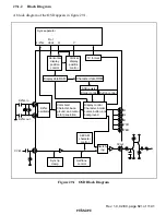
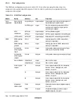
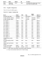
The OSD pin configuration is shown in table 29.1. Even when not using the data slicer, the
composite video signal should be input to Cvin2 in order to perform sync separation from the
composite video signal.
Table 29.1
OSD Pin Configuration
Block
Name
Abbrev.
I/O
Function
Csync/Hsync
Input/output
Composite sync signal input/output or
horizontal sync signal input
Sync signal
input/output
VLPF/Vsync
Input
Pin for connecting external LPF for
vertical sync signal or input pin for
vertical sync signal
AFCosc
Input/output
AFC oscillation signal
AFC
oscillation
AFCpc
Input/output
AFC by-pass capacitor connecting pin
Sync
separator
LPF for AFC
AFCLPF
Input/output
External LPF connecting pin for AFC
OSD analog
power
OVcc
Input
Analog power for OSD, data slicer,
and sync separator
OSD analog
ground
OVss
Input
Analog ground for OSD, data slicer,
and sync separator
Composite
video signal
input
CVin1
Input
Composite video signal input (2 Vpp,
with a sync tip clamp circuit)
Composite
video signal
output
CVout
Output
Composite video signal output (2 Vpp)
4fsc/2fscin
Input
4fsc or 2fsc input
fsc oscillation
4fsc/2fscout
Output
4fsc or 2fsc output
R
Output
Color signal output (R) for character,
border, cursor, background, and
button, or a port
G
Output
Color signal output (G) for character,
border, cursor, background, and
button, or a port
Color signal
output
B
Output
Color signal output (B) for character,
border, cursor, background, and
button, or a port
YCO
Output
Character data output (digital output),
or a port
OSD
Character
data output
YBO
Output
Character display position output
(digital output), or a port

