Rev. 1.0, 02/00, page 137 of 1141
7.3.3
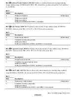
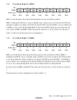
Erase Block Register 1 (EBR1)
7
EB7
0
R/W
6
EB6
0
R/W
5
EB5
0
R/W
4
EB4
0
R/W
3
EB3
0
R/W
0
EB0
0
R/W
2
EB2
0
R/W
1
EB1
0
R/W
Bit
EBR2
Initial value
R/W
:
:
:
:
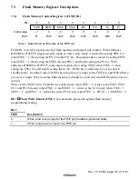
EBR1 is an 8-bit register that specify the flash memory erase area block by block.
EBR1 is initialized to H'00 by a reset, in standby mode, when a low level is input to the FWE pin,
and when a high level is input to the FWE pin and the SWE1 bit in FLMCR1 is not set. When a bit
in EBR1 is set to 1, the corresponding block can be erased. Other blocks are erase-protected. Set
only one bit in EBR1 and EBR2. More than one bit cannot be set. If set, all bits are cleared to 0.
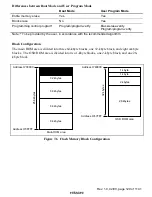
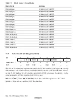
Table 7.3 shows the flash memory block configuration.
7.3.4
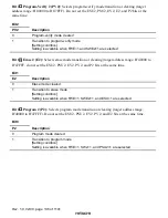
Erase Block Register 2 (EBR2)
7
EB15
0
R/W
6
EB14
0
R/W
5
EB13
0
R/W
4
EB12
0
R/W
3
EB11
0
R/W
0
EB8
0
R/W
2
EB10
0
R/W
1
EB9
0
R/W
Bit
EBR2
Initial value
R/W
:
:
:
:
EBR2 is an 8-bit register that specify the flash memory erase area block by block; EBR2 is
initialized to H'00 by a reset, is standby mode, and when a low level is input to the FWE pin. Bits
3 to 0 are initialized to 0 when a high level is input to the FWE pin and the SWE1 in FLMCR1 is
not set. Bits7 to 4 are initialized to 0 when the SWE2 in FLMCR2 is not set. When a bit in EBR2
is set to 1, the corresponding block can be erased. Other blocks are erase-protected.
Set only one bit in EBR1 and EBR2. More than one bit cannot be set. If set, all bits are cleared to
0.
The flash memory block configuration is shown in table 7.3.

