Rev. 1.0, 02/00, page 76 of 1141
4.2.3
Timer Register A (TMA)
0
0
1
0
R/W
2
0
3
0
4
1
5
—
—
1
6
0
7
R/W
R/W
R/W
R/W
TMA3
R/W
TMA2
R/W
TMAIE
0
R/(W)*
TMAOV
TMA1
TMA0
Bit :
Initial value :
R/W :
Note: *
Only 0 can be written, to clear the flag.
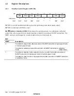
The timer register A (TMA) controls timer A interrupts and selects input clock.
Only bit 3 is explained here. For details of other bits, see section 11.2.1, Timer Mode Register A.
TMA is a readable/writable register which is initialized to H'30 by a reset.
Bit 3
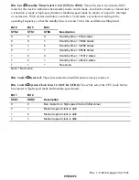
Clock Source, Prescaler Select (TMA3): Selects timer A clock source between PSS and
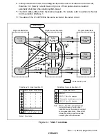
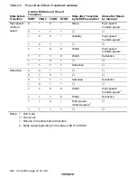
PSW. It also controls transition operation to the power-down mode. The operation mode to which
the MCU is transited after SLEEP instruction execution is determined by the combination with
other control bits.
For details, see the description of clock select 2 to 0 in section 11.2.1, Timer Mode Register A.
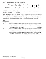
Bit 3
TMA3
Description
0
•
Timer A counts
φ
-based prescaler (PSS) divided clock pulses
•
When a SLEEP instruction is executed in high-speed mode or medium-speed
mode, a transition is made to sleep mode or software standby mode
(Initial value)
1
•
Timer A counts
φ
w-based prescaler (PSW) divided clock pulses
•
When a SLEEP instruction is executed in high-speed mode or medium-speed
mode, a transition is made to sleep mode, watch mode, or subactive mode
•
When a SLEEP instruction is executed in subactive mode, a transition is made
to subsleep mode, watch mode, or high-speed mode

