Rev. 1.0, 02/00, page 370 of 1141
19.1.2
Block Diagram
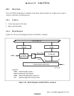
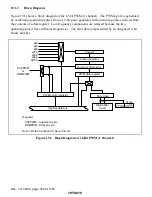
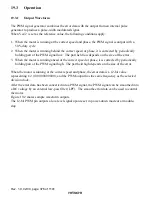
Figure 19.1 shows a block diagram of the 12-bit PWM (1 channel). The PWM signal is generated
by combining quantizing pulses from a 12-bit pulse generator with quantizing pulses derived from
the contents of a data register. Low-frequency components are reduced because the two
quantizing pulses have different frequencies. The error data is represented by an unsigned 12-bit
binary number.
Internal data bus
[Legend]
Note:
*
Refer to section 26, Servo Circuit.
CAPPWM
or
DRMPWM
CAPPWM
φ
/2
φ
/4
φ
/8
φ
/16
φ
/32
φ
/64
φ
/128
DRMPWM
: Capstan mix pin
: Drum mix pin
PWM control register
Digital filter
circuit
Error data
PTON
PWM data register
Output control circuit
Pulse generator
Counter
DFUCR
CP/
Figure 19.1 Block Diagram of 12-Bit PWM (1 channel)

