Rev. 1.0, 02/00, page 130 of 1141
7.2.4
Pin Configuration
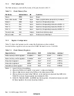
The flash memory is controlled by means of the pins shown in table 7.1.
Table 7.1
Flash Memory Pins
Pin Name
Abbreviation
I/O
Function
Reset
5(6
Input
Reset
Flash write enable
FWE
Input
Flash program/erase protection by hardware
Mode 0
MD0
Input
Sets this LSI operating mode
Port 12
P12
Input
Sets this LSI operating mode when MD0 = 0
Port 13
P13
Input
Sets this LSI operating mode when MD0 = 0
Port 14
P14
Input
Sets this LSI operating mode when MD0 = 0
Transmit data
SO1
Output
Serial transmit data output
Receive data
SI1
Input
Serial receive data input
7.2.5
Register Configuration
Table 7.2 shows the registers used to control the flash memory when enabled.
In order for these registers to be accessed, the FLSHE bit must be set to 1 in STCR.
Table 7.2
Flash Memory Registers
Register Name
Abbreviation
R/W
Initial Value
Address
*
1
Flash memory control register 1
FLMCR1
*
5
R/W
*
2
H'00
*
3
H'FFF8
Flash memory control register 2
FLMCR2
*
5
R/W
*
2
H'00
*
4
H'FFF9
Erase block register 1
EBR1
*
5
R/W
*
2
H'00
*
4
H'FFFA
Erase block register 2
EBR2
*
5
R/W
*
2
H'00
*
4
H'FFFB
Serial timer control register
STCR
R/W
H'00
H'FFEE
Notes: 1. Lower 16 bits of the address.
2. When the FWE bit in FLMCR1 is not set at 1, writes are disabled.
3. When a high level is input to the FWE pin, the initial value is H'80.
4. When a low level is input to the FWE pin, or if a high level is input and the SWE bit in
FLMCR1 is not set, these registers are initialized to H'00.
5. FLMCR1, FLMCR2, EBR1, and EBR2 are 8-bit registers. Only byte accesses are valid
for these registers, the access requiring 2 states.


