Rev. 1.0, 02/00, page 866 of 1141
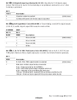
Bit 2
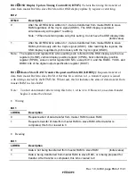
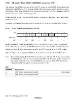
Monitor Signal Switching Bit (CRSEL): Selects whether a clock run-in detection
window signal or a start bit detection window signal is output. This bit setting is valid when DSEL
is 1, so that pins are used as data slicer internal monitor signal outputs.
Bit 2
CRSEL
Description
0
Clock run-in detection window signal output is selected
(Initial value)
1
Start bit detection window signal output is selected
For information on slice data and the sampling clock, refer to section 28.2.2, Slice Line Setting
Registers 1 to 4. For details on the clock run-in detection window signal, start bit detection
window signal, external Hsync signal (AFCH), and external Vsync signal (AFCV), refer to section
27, Sync Separator for OSD and Data Slicer.
Bit 1
Reserved: Cannot be modified and is always read as 1.
Bit 0
Reserved: Always read as 0. When 1 is written to this bit, correct operation is not
guaranteed.
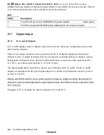
29.7.4
Module Stop Control Register (MTSTPCR)
7
1
R/W
MSTP
15
MSTP
14
MSTP
13
MSTP
12
MSTP
11
MSTP
10
MSTP
9
MSTP
8
MSTP
7
MSTP
6
MSTP
5
MSTP
4
MSTP
3
MSTP
2
MSTP
1
MSTP
0
6
1
R/W
5
4
1
R/W
MSTPCRH
MSTPCRL
1
R/W
3
1
R/W
2
1
R/W
1
1
R/W
0
1
R/W
7
1
R/W
6
1
R/W
5
1
R/W
4
1
R/W
3
1
R/W
2
1
R/W
1
1
R/W
0
1
R/W
Bit:
Initial value:
R/W:
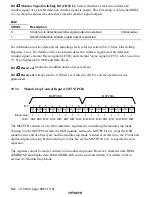
The MSTPCR consists of two 8-bit read/write registers for controlling the module stop mode.
Writing 0 to the MSTP0 bit starts the OSD module; setting the MSTP0 bit to 1 stops the OSD
module at the end of a bus cycle and the module stop mode is entered. At this time, the CVout and
digital outputs also stop. Before writing 0 to this bit, set the MSTP9 bit to 0, to operate the sync
separator.
The registers cannot be read or written to in module stop mode. However, character data ROM
(OSDROM) and display data RAM (OSDRAM) can be read and written. For details, refer to
section 4.5, Module Stop Mode.

