Rev. 1.0, 02/00, page 718 of 1141
26.14
Frequency Dividers
26.14.1
Overview
On-chip frequency dividers are provided for the pulse signal picked up from the control track
during playback (the PB-CTL signal), and the pulse signal received from the capstan motor (CFG
signal). The CTL frequency divider generates a CTL divided control signal (DVCTL) from the
PB-CTL signal, for use in capstan phase control during high-speed search, for example. The CFG
frequency divider generates two divided CFG signals (DVCFG for speed control and DVCFG2 for
phase control) from the CFG signal. The DFG noise canceller is a circuit which considers signal
less than 2
φ
as noise and mask it.
26.14.2
CTL Frequency Divider
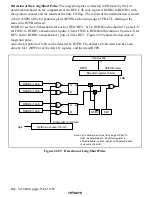
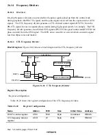
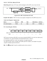
Block Diagram: Figure 26.63 shows a block diagram of the CTL frequency divider.
EXCTL
PB-CTL
↑
↑
,
↓
DVCTL
UDF
R/W
W
(8 bits)
R/W
Internal bus
CEX
CTL division register
Down counter (8 bits)
CEG
Edge
detector
CTVC
CTLR
CTVC
Figure 26.63 CTL Frequency Divider
Register Description
−
Register configuration
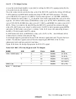
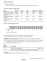
Table 26.22 shows the register configuration of the CTL frequency dividers.
Table 26.22
Register Configuration
Name
Abbrev.
R/W
Size
Initial Value
Address
DVCTL control register
CTVC
R/W
Byte
Undefined
H'D098
CTL frequency division
register
CTLR
W
Byte
H'00
H'D099

