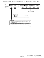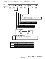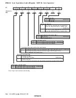
Rev. 1.0, 02/00, page 1076 of 1141
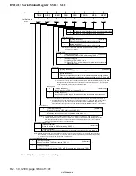
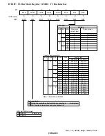
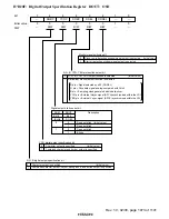
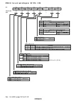
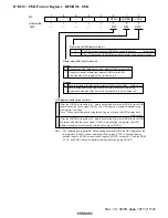
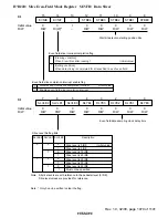
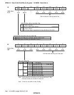
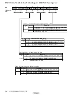
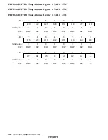
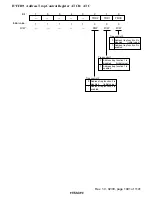
H'D212: OSD Format Register DFORM: OSD
8
0
9
0
R/W
10
0
—
11
0
12
0
R/W
0
R/W
13
15
FSCIN
FSCEXT
—
OSDVE
OSDVF
0
R/W
TVM2
14
0
R/W
TVM1
R/(W)*
1
R/W
TVM0
Notes: 1. Only 0 can be written to clear the flag.
2. The 4fsc and 2fsc frequencies for SECAM do not conform to the SECAM TV format
specifications.
Bit 15
Bit 14
Bit 13
Bit 12
Description
TVM2
TVM1
TVM0
FSCIN
TV Format
4fsc (MHz) 2fsc (MHz)
0
0
0
0
M/NTSC
14.31818
—
1
—
—
7.15909
0
17.734475
0
0
1
4.43-NTSC
(17.734470)
1
—
8.867235
(8.867238)
0
1
0
0
M/PAL
14.302446
—
(14.302444)
1
—
7.15122298
0
1
1
0/1
Must not be specified
1
0
0
0
N/PAL
14.328225
(14.28244) —
1
—
7.1641125
1
0
1
0/1
Must not be specified
0
B,G,H/PAL
17.734475
—
1
1
0
I/PAL
(17.734476)
1
D,K/PAL
—
8.867235
(8.867238)
0
B,G,H/SECAM*
2
17.734475
—
1
1
1
L/SECAM
(17.734470)
1
D,K,K1/SECAM
—
8.867235
(8.867238)
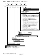
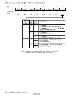
OSDV interrupt enable bit
0
1
4/2fsc external input select bit
0
1
4/2fsc input select bit
TV format select bits
0
1
OSDV interrupt flag
:
:
:
0
1
Bit
Initial value
R/W
—
4fsc input is selected (Initial value)
2fsc input is selected
4/2fsc oscillator uses a crystal oscillator (Initial value)
4/2fsc uses a dedicated amplifier circuit for external clock signal input
The OSDV interrupt is disabled (Initial value)
The OSDV interrupt is enabled
[Clearing condition]
When 0 is written after reading 1 (Initial value)
[Setting condition]
When OSD detects the Vsync signal


