Rev. 1.0, 02/00, page 731 of 1141
26.14.4
DFG Noise Removal Circuit
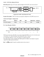
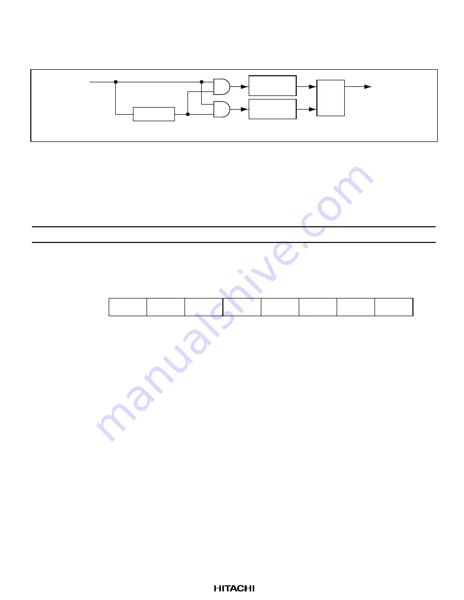
Block Diagram: Figure 26.70 shows the block diagram of the DFG noise removal circuit.
Rising edge
detection
Delay circuit
DFG
S
Q
R
NCDFG
delay = 2
φ
Falling edge
detection
Figure 26.70 DFG Noise Removal Circuit
Register Description: Table 26.24 shows the register configuration of the DFG mask circuit.
Table 26.24 Register Configuration
Name
Abbrev.
R/W
Size
Initial Value
Address
FG control register
FGCR
W
Byte
H'FE
H'D09E
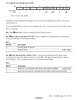
FG Control Register (FGCR)
0
0
1
1
2
1
3
1
4
1
5
1
6
1
7
—
—
—
—
—
—
—
—
—
—
—
—
—
—
W
DRF
1
Bit :
Initial value :
R/W :
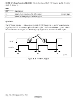
FGCR selects the edge of the DFG noise removal signal (NCDFG) to be sent to the drum speed
error detector. If a read is attempted, an undetermined value is read out.
It is initialized to H'FE by a reset, or in stand-by or module stop mode.
The edge selection circuit is located in the drum speed error detector, and outputs the register
output to the drum speed error detector.
Bits 7 to 1
Reserved: Cannot be modified and are always read as 1.


