Rev. 1.0, 02/00, page 592 of 1141
26.4.4
Register Configuration
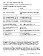
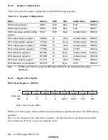
Table 26.6 shows the register configuration of the HSW timing generator.
Table 26.6
Register Configuration
Name
Abbrev.
R/W
Size
Initial Value
Address
HSW mode register 1
HSM1
R/W
Byte
H'30
H'D060
HSW mode register 2
HSM2
R/W
Byte
H'00
H'D061
HSW loop stage number setting
register
HSLP
R/W
Byte
Undetermined
H'D062
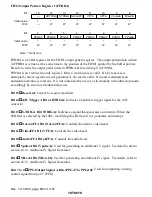
FIFO output pattern register 1
FPDRA
W
Word
Undetermined
H'D064
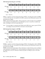
FIFO timing pattern register 1*
FTPRA
W
Word
Undetermined
H'D066
FIFO output pattern register 2
FPDRB
W
Word
Undetermined
H'D068
FIFO timing pattern register 2
FTPRB
W
Word
H'FFFF
H'D06A
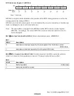
DFG reference register 1*
DFCRA
W
Byte
Undetermined
H'D06C
DFG reference register 2
DFCRB
W
Byte
Undetermined
H'D06D
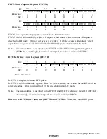
FIFO timer capture register*
FTCTR
R
Word
H'0000
H'D066
DFG reference count register*
DFCTR
R
Byte
H'E0
H'D06C
Note:
*
FTPRA and FTCTR, as well as DFCRA and DFCTR, are allocated to the same
addresses.
26.4.5
Register Description
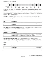
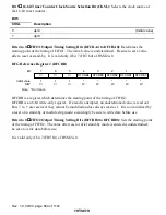
HSW Mode Register 1 (HSM1)
0
0
1
0
R/W
2
0
R/(W)*
3
0
4
1
R
1
R
5
6
0
7
EMPA
OVWB
OVWA
CLRB
CLRA
0
R
FLB
R/W
R/(W)*
R
FLA
EMPB
Bit :
Initial value :
R/W :
Note: * Only 0 can be written
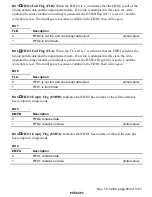
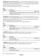
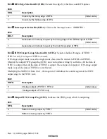
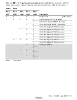
HSM1 is an 8-bit register which confirms and determines the operational state of the HSW timing
generator.
Bits 7 to 4 are read-only bits, and write is disabled. All the other bits accept both read and write.
It is initialized to H'30 by a reset or in stand-by mode.


