Rev. 1.0, 02/00, page 330 of 1141
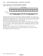
16.2.7
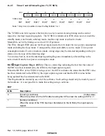
Timer Output Comparing Control Register (TOCR)
0
0
1
0
2
0
3
0
4
0
5
0
6
0
7
R/W
R/W
ICSC
0
R/W
ICSB
R/W
OSRS
R/W
ICSD
R/W
OEB
R/W
OEA
OLVLB
R/W
OLVLA
Bit :
Initial value :
R/W :
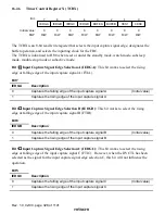
The TOCR is an 8-bit read/write register that select input capture signals and output comparing
output level, permits output comparing outputs, and controls switching over of the access of the
OCRA and OCRB. See section 16.2.4, Timer Interrupt Enabling Register (TIER) regarding the
input capture inputs A.
The TOCR is initialized to H'00 when reset or under the standby mode, watch mode, subsleep
mode, module stop mode or subactive mode.
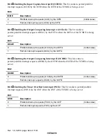
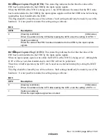
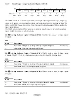
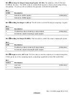
Bit 7
Selecting the Input Capture B Signals (ICSB): This bit works to select the input capture
B signals.
Bit 7
ICSB
Description
0
Selects the FTIB pin for inputting of the input capture B signals
(Initial value)
1
Selects the VD as the input capture B signals
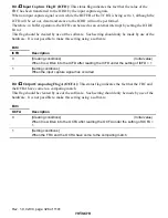
Bit 6
Selecting the Input Capture C Signals (ICSC): This bit works to select the input capture
C signals. The DVCTL is the edge detecting pulse selected by the CTL dividing timer.
Bit 6
ICSC
Description
0
Selects the FTIC pin for inputting of the input capture C signals
(Initial value)
1
Selects the DVCTL as the input capture C signals
Bit 5
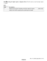
Selecting the Input Capture D Signals (ICSD): This bit works to select the input capture
D signals.
Bit 5
ICSD
Description
0
Selects the FTID pin for inputting of the input capture D signals
(Initial value)
1
Selects the NHSW as the input capture D signals


